Processor Design Project
This is the homepage for the Processor Design Project. You can find most course information here.
This course is part of the CESE masters programme. This course is a continuation of the curriculum of Computer Engineering (CESE4130) and Modern Computer Architecture (CESE4085).
Notice of Changes
This course will be SIGNIFICANTLY changed this year (2025), and the information on this page is no longer 100% correct. It is currently being updated.
Project Overview
In this course, you will be enhancing an RISCV-based CPU and its associated LLVM toolchain for the task of Advanced Encryption Standard (AES) encoding in groups of four (4). First, you will extend the basic CPU (named RISCY) with your own implementation of the AES instructions, aes32esi and aes32esmi. Thereafter, you will apply yhe standard LLVM loop unrolling pass for the aes32esmi instruction. All additional improvements and optimisations of the AES enhanced RISCY CPU and LLVM compiler are up to your group. Please remember that you have to evaluate your new design for the intended improvements and quantitatively compare against a state-of-the-art and baseline methohds. Your designs will be targeting an FPGA board. To facilitate you doing so, you will receive:
- A Git repository which is initially the same for groups and includes the basic RISCV processor (RISCY) Verilog code, the LLVM source files and a simple benchmark (a software implementation of AES). Each group has access to its own repository for further extentions.
- All necessary tools and files required for simulation and FPGA implementation are available on a design server. Each group has an account on the server for remote access.
- This website, detailing the project assignment and the simulation general flow and toolset.
Schedule
| Date | Activity |
|---|---|
| April 23rd in Pulse Hall 10 | Kickoff Meeting at 13:45 |
| Every Thursday afternoon (except public holidays) | Q&A Lab in EWI Halls H,G,K,L and M from 13:45 to 17.45 |
| May 2 | Intermediate Report Submission |
| May 9 | Feedback on your Intermediate Report |
| June 20 | Final Report and Project Submission |
Getting Started
- Form a Group of four student and register it in Brightspace!
- Carefully read the First Phase section. It contains information on what is expected in the first two weeks of the project.
- Any additional questions on how to set up your project, and other support will be provided at the weekly labs!
- In Frequently Asked Questions we are collecting some frequent questions. Please contribute in the labs! (NEED UPDATE)
Grading Procedure
The projects functionality will be verified and checked for (including between groups) plagiarism.
If the project is not functional you DO NOT pass the course. Plagiarism can also make you fail.
The final score for the project is determined based on the following criteria:
The evaluation method and criteria are changed this year (2025)! Soon, the new rules will be available.
Staff
The course will be led by Motta Taouil and Georgi Gaydadjiev, with assistance of Carlo Galuzzi, Stephan Wong and Mahmood Naderan-Tahan .
Additionally, a team of six TAs will be helping us too:
Contact
- For reaching the entire team and general enquiries, please use CESE4040.2025@tudelft.nl. Please use “CESE4040HelpDesk:" as the beginning of your subject line.
Project Setup
In this section, you will find all information about connecting to the server, the RISCY architecture, loading the project on Vivado and generating FPGA bit stream.
1. Server
Once the groups are formed an account per group will be provided to work directly in the server. Each group has access to its own repository on Gitlab hosted by TU Delft. To be able to clone the repository on the server, please setup an access token on the Gitlab website. You can read the official document for more information or follow the steps below:
Note: Setting up a personal access token must be done by each group member independently.
-
On your laptop, open a web browser and go to https://gitlab.ewi.tudelft.nl and login with your NetID.
-
Click on your avatar and navigate to Edit Profile and then Access Tokens.
-
Click on Add new token, give it a name and select check boxes on you choice (check all for simplicity) and clock on Create personal access token.
-
After that you will see a green box showing your access token. Please keep that in a safe place because if you leave the page, you are no longer to see the token again.
Now it is time to setup access to the server. Each project group uses one account on the development server. Each group in the Brightspace has a locker which contains the server credentials. Use username and password to access the following server:
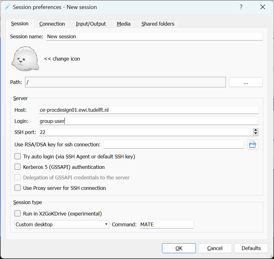
ce-procdesign01.ewi.tudelft.nl
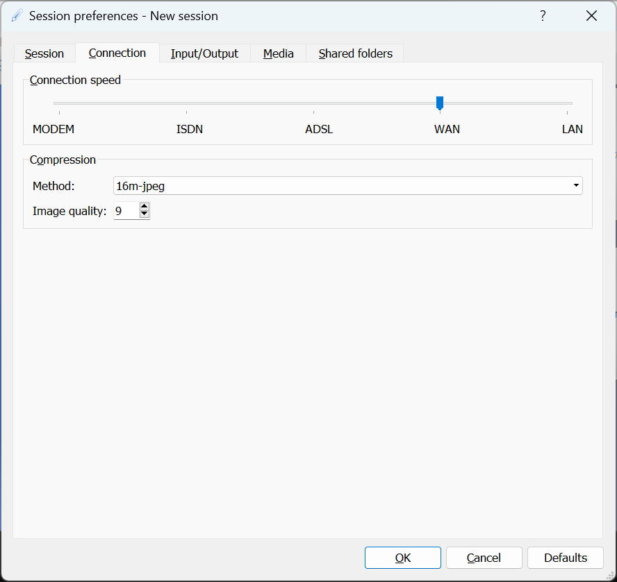
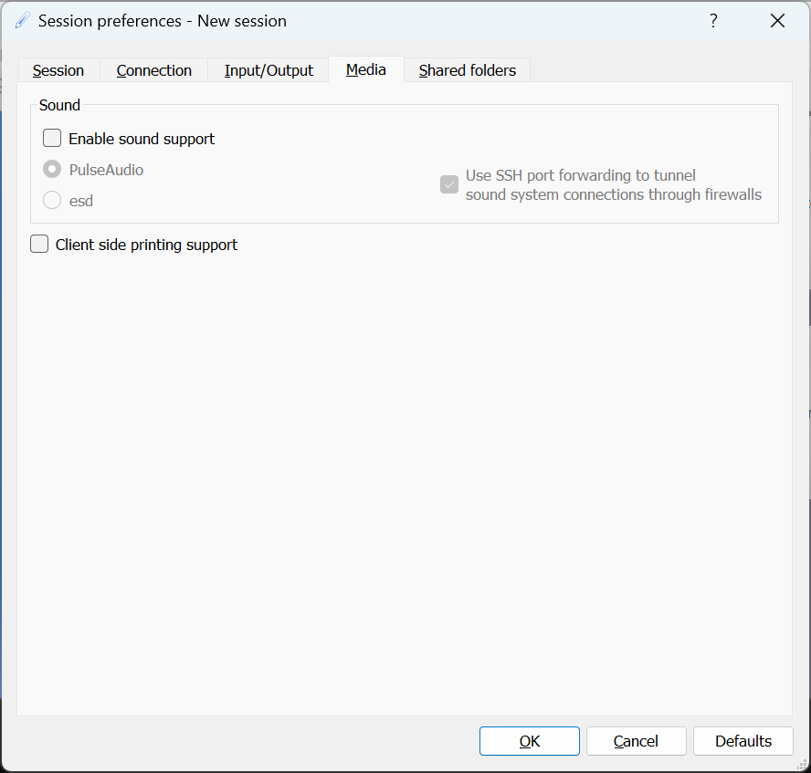
Please note that, if you want to connect to the server from outside of the campus network, you have to use EduVPN. The server provides graphical interface to a Linux based operating system. Therefore, the recommended client software is X2GO. Please download and install the software and make sure that you have carefully read the QCE guide to setup the connection. See Figures 1, 2 and 3 for more information. Please use the proper user name as mentioned earlier.
 |
|---|
| Figure 1. Session window |
 |
|---|
| Figure 2. Connection menu |
 |
|---|
| Figure 3. Media menu |
Note: It is important to note that when you intend to leave the session, you should always logout from the GUI. Do not close the client window as it will be still running on background and uses unnecessary resources. Administrative settings will terminate any stale session after four hours.
Note: For simultanous multiple connections, please see this page.
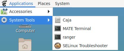
Once you logged in to the session, open a terminal as shown in Figure 4 and clone your repository.
 |
|---|
| Figure 4. Launching terminal |
The steps are described below:
-
Run
git clone https://gitlab.ewi.tudelft.nl/qce/computer-engineering/computer-engineering/courses/pdp-processor-design-project/student-work/2024-2025/pdp-project-XXwhereXXis your group number, 01, 02, ... and 24. -
When asked for user name, use your NetID and not the
group-XX. -
When asked for password, use you personal access token.
If the operation is successful, you will see the cloning progress and after that by running ls command you should see pdp-project-XX folder.
You can edit sources files via one of the following options:
- Directly from the server using vim or Gedit.
- Remotely from your computer using VSCode and the ssh plugin. See this guide for more information.
There exists only one user name and password on the server for each group. However, groups members want to connect to different desktop session while working on different programs. There are various ways to achieve that, here we explain two methods: 1) Using remote ssh and 2) Using X2GO client.
Using Remote SSH
You can always connect to the server via ssh command and enable X11 forwarding to see the application GUI, e.g. Vivado. On Linux terminal, or Windows Linux Subsystem (WSL) terminal, use
ssh -X ce-procdesign01.ewi.tudelft.nl
and provide the user name and password of your group. You are then able to launch Vivado but depending on the connection speed, it may be slow.
Using X2GO client
With X2GO client, the first member who connects to the server will receive the desktop environment instantly. However, the second member will be notified about a running desktop. At this point, it is possbile to click on the New button and request a new desktop. Please see the screen shots below for further information.
Please note that, some applications use their own lock to prevent running multiple instances. That limit unfortunately is imposed by the application.
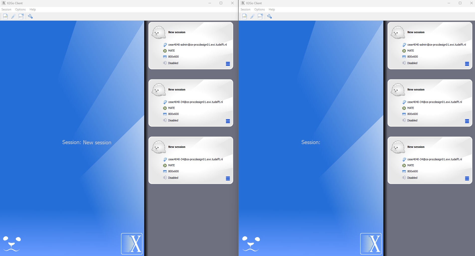
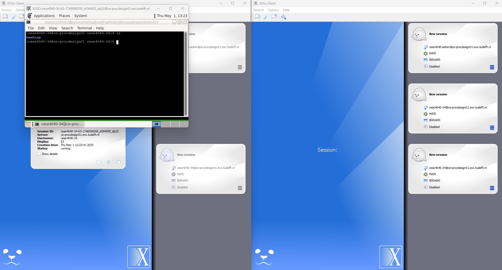
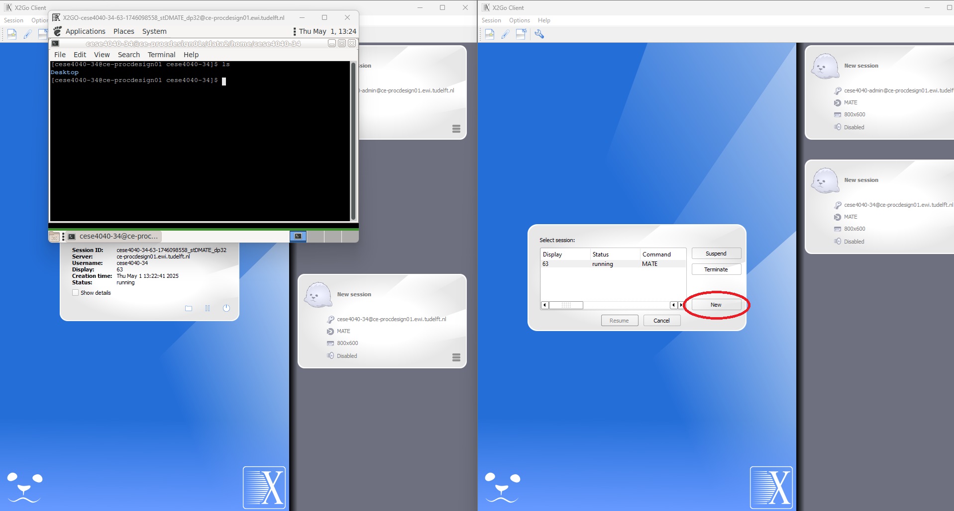
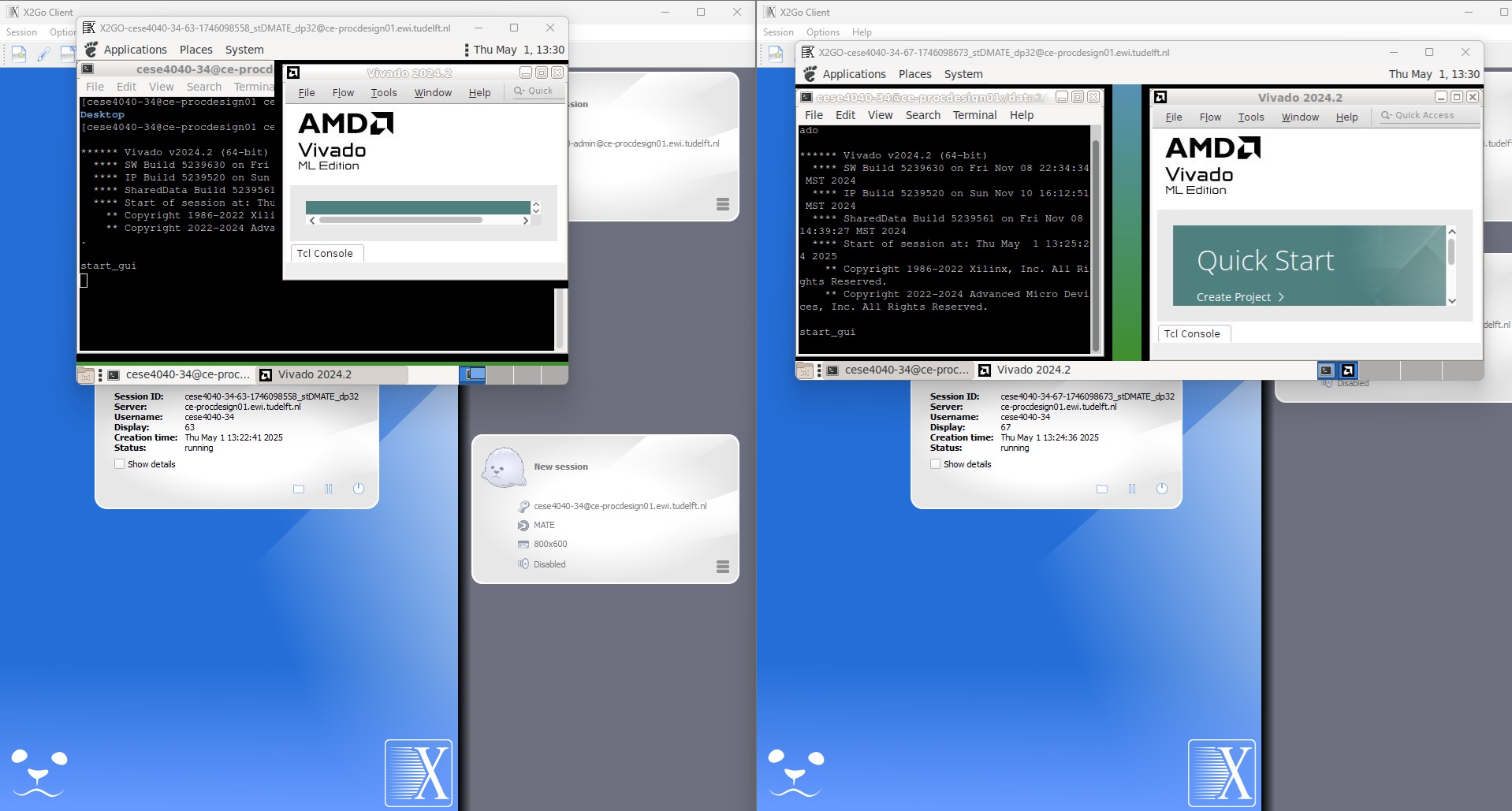
Figure 1. Multiple desktop session with X2GO
2. RISCY Core
RI5CY1 is a small four-stage RISC-V core implementation. It fully implements the RV32I instruction set, the multiply instruction from RV32M and many custom instruction set extensions, namely RV32IMFC, that improve its performance for signal processing applications. The core was developed as part of the PULP platform for energy-efficient computing. Figure 5 shows the datapath of RI5CY core. More information can be found in the manual.
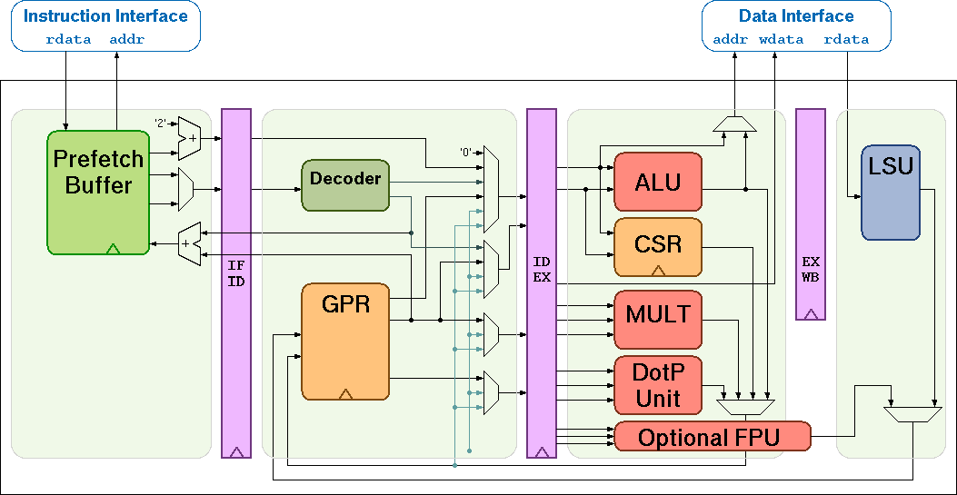 |
|---|
| Figure 5. RIS5CY datapath |
The RTL source files for the RISCY version you will use as the starting point for your project can be found in the course directory in the server, alternatively they can also be found in the gitlab repository (TBD link).
-
In this document, RISCY and RI5CY are used interchangeably. ↩
3. PDP Project
3.1 Vivado
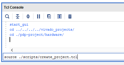
To launch the Vivado Software, open a terminal and type vivado. For your convenience, several scripts are provided with the base RISCY repository mentioned earlier. These scripts can be executed directly from the Vivado’s TCL console. To do so, first change your directory to pdp-project/hardware/ then use source command as shown Figure 6.
 |
|---|
| Figure 6. TCL Console |
Alternatively, you can execute the script by invoking vivado command vivado -mode batch -source <your_Tcl_script> with the same effect as Figure 6.
3.1.1 Project Creation
A dedicated script to generate the base FPGA system that will be used for simulation and implementation. The script is located at pdp-project/hardware/scripts/create_project.tcl. After running this script, your project is loaded in Vivado as shown in Figure 7.
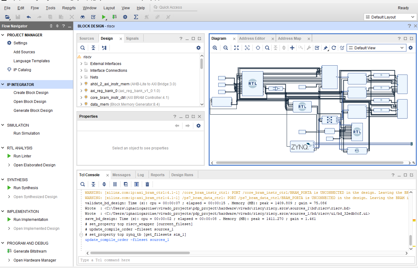 |
|---|
| Figure 7. Loaded project in Vivado |
Under the Sources tab, you can find both the RTL source files, constraints and simulation sources, as shown in Figure 8. Selected top levels, often referred to as tops, are shown in bold font. There are two tops in every design, one for the Design Sources, used for synthesis and implementation, and one for the Simulation Sources, used for simulation. More information is provided next.
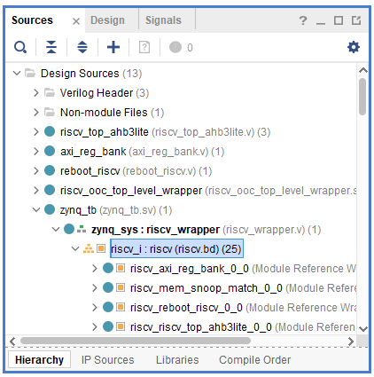
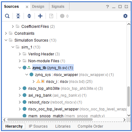
Figure 8. Sources tab
3.1.2 Top Level Design
The design top level source is a block diagram autogenerated using one of the provided TCL scripts in pdp-project/hardware/scripts/generate_fpga_bd.tcl and is shown in Figure 9.
 |
|---|
| Figure 9. Block diagram of the design |
This block diagram shows what will be synthesized and loaded on the FPGA. It consists of the following relevant blocks/modules:
riscv_top_ahb3lite: Wrapper around the top level of RISCY, it includes the interfacing IPs1 used to connect the core to on-chip FPGA SRAM memory blocks, also referred to as BRAMs.instr_mem: Dual port BRAM containing the instructions executed by your processor.data_mem: Dual port BRAM containing the data.procesing_system7: Instance of the hardened ARM core available in the FPGA device, used to generate the clock of your processor design and to write/read data to and from the other IPs, e.g. program and data memories, of the design via an AXI bus.mem_snoop_match: Small module in charge of snooping the data memory interface, configured to spot the end sequence,0xDEADBEEF, at address0x2000. Also counts the clock cycles since its clock enable input is asserted (connected to fetch enable) until the end sequence is found.reboot_riscv: Control block used in the design to assert/deassert the fetch enable and reboot signals connected to the core.axi_reg_bank: Register bank used to be able to access PL2 signals via AXI from the processing system.- Interconection blocks:
Smartconnect(used to access from a single processing system AXI master three AXI slaves), bram controllers and AHB3-Lite to AXI adaptor (needed to interface between different protocols used by Vivado IPs or the core and the native BRAM interface), and so on. shift_addr: Used given that the generated BRAMs by vivado are addressed per word, instead of per byte as AXI and our core do. Since the word width of the BRAMs is 4-bytes, we just shift the input address by 2 bits.
3.1.3 Top Level Simulation
System simulation:
The testbench source file can be found at pdp-project/hardware/src/simulation/zynq_tb.sv.
The testbench just generates the necessary clock and reset signals, connects them to the top level of the design, and performs some reads/writes via the processing_system AXI.
Both instructions and initial data are preloaded into the BRAMs by the generate_fpga_bd.tcl script, where you can check that the memory initialization files being loaded are code.coe and data.coe and should be placed in pdp-project/hardware/src/sw/mem_files.
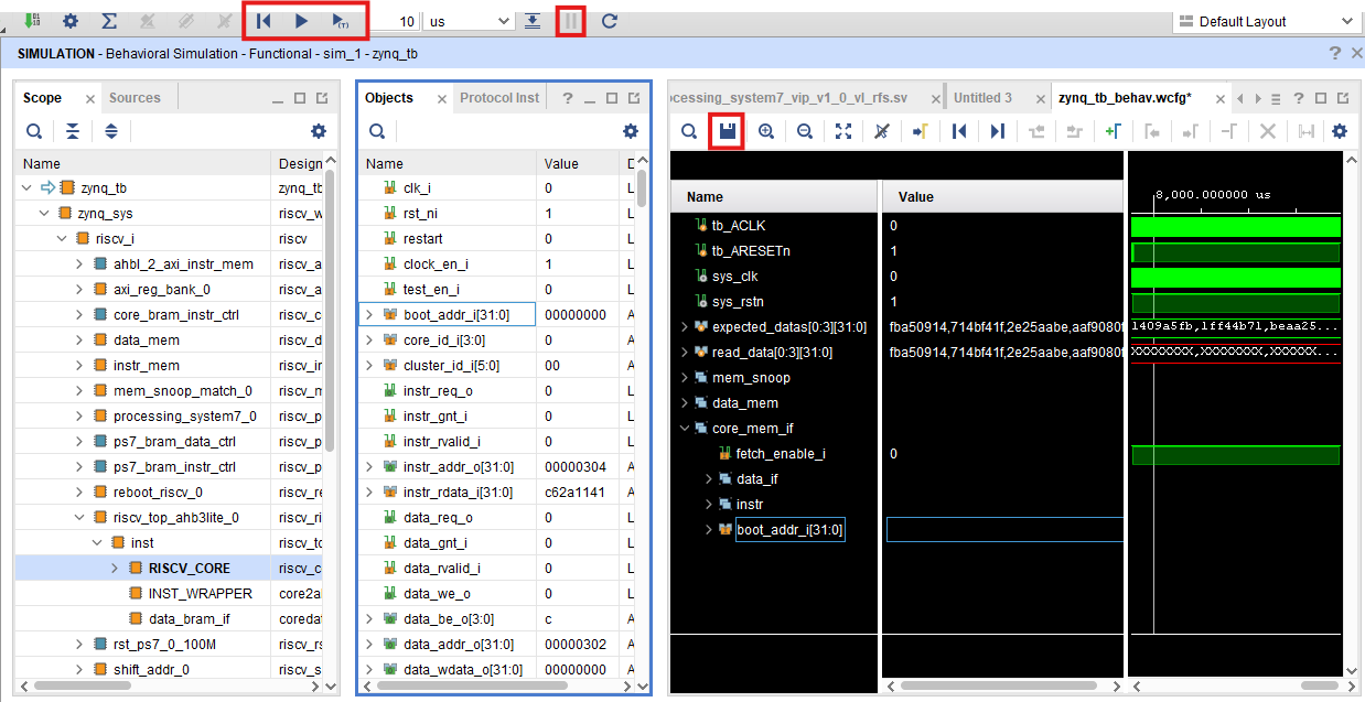
A script has been provided to run the simulations and preload a selection of waveforms. To use it just run source ./scripts/run_simulation.tcl. It will take around a minute to elaborate all the project sources and then it will run the simulation. Depending on the code being executed in the core it will take more or less than four minutes to simulate the baseline software AES encryption. Once the simulation finishes your Vivado window will look like Figure 10.
 |
|---|
| Figure 10. Simulation output |
The waveform window with the preselected signals is highlighted in red. You can always add or modify the selected signals and save your view. This way the next time you run a simulation with the script it will show your own version.
If you add signals that were not selected before running the simulation, you will only be able to see their final value. Click on Restart, and then on Run as shown in Figure 11.
 |
|---|
| Figure 11. Waveform output |
You can always stop the simulation at whatever point you want by using the Pause button. The console output of the base project by the end of the simulation is shown in Figure 12.
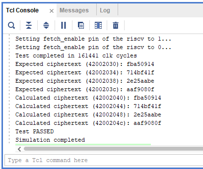 |
|---|
| Figure 12. Console output after simulation finishes |
Module simulation:
Only testbench files and scripts for system level simulation are provided (core + memories), if lower-level testing is required (i.e: modules that are part of the core) you are expected to implement all of the required files (testbench, testcases, scripts) needed to verify and debug your project yourself.
3.1.4 Synthesis and Implementation
If you just want to verify your changes to the RISCY core or how does the resource utilization changed, it is recommended to just run an OOC3 synthesis as it will be faster than running synthesis on the entire project.
To run the OOC synthesis just open a new vivado window, change directory to the hardware directory and then source this script pdp-project/hardware/scripts/create_project_ooc_synth.tcl. This script will also save the results in pdp-project/hardware/vivado/ooc_riscy/ooc_riscy.runs/ooc_synth/. In Vivado the reports look like Figure 13.
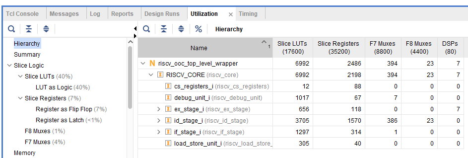
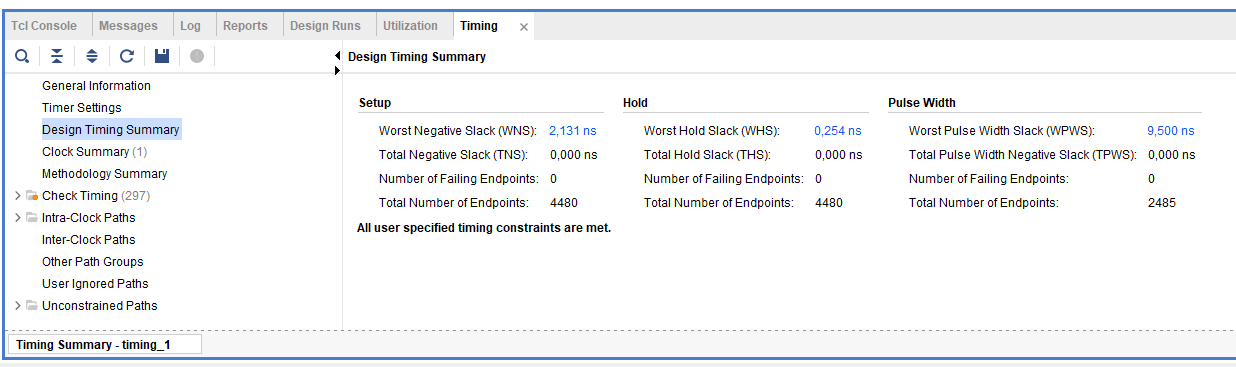
Figure 13. Timing and utilization reports
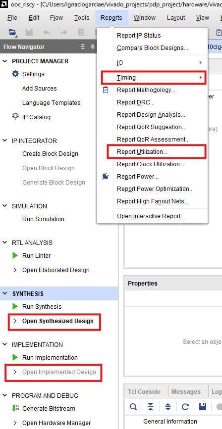
To generate these reports manually for any design, just click on Open Synthesized Design or Open Implemented Design depending on the step you got and then on Reports->Timing or Reports->Report Utilization for Utilization/Timing as shown in Figure 14.
 |
|---|
| Figure 14. Reports menu |
If you want to run synthesis or implementation for the full project manually, you can always use the Run Synthesis or Run Implementation options.
3.1.5 Bitstream Generation
You can generate the FPGA bitstream from your RISCY project by just sourcing pdp-project/hardware/scripts/run_synth_impl.tcl. You can also create the project and generate the bitstream with a single script by sourcing pdp-project/hardware/scripts/gen_bitstream.tcl from a new vivado window. You can find the generated bitstream at pdp-project/hardware/vivado/riscy/riscy.runs/impl_1/riscv_wrapper.bit.
Note: It is always advised to generate timing and utilization resources of the implemented design before trying to use the bitstream on the board, this way you can spot any possible timing violations or RTL getting optimized away.
3.2 Application: AES Code (C)
The baseline software implementation of the AES encryption is provided in C and can be found in pdp-project/software/main.c.
This source file contains all the functions used to perform the encryption, the initial text, the key to be used and the expected ciphertext. For example, the input text “Hello, World!000” and the key “cese4040password” are hardcoded in the program.
The main function of this C file just performs the encryption of the input text, writes the ciphertext and the expected ciphertext to a given address, checks the output and writes either 0xBAAAAAAD or 0xCADEBABE depending on if the ciphertext matches expected, and writes the end sequence 0xDEADBEEF detected by the mem_snoop module on the FPGA to a specific address 0x0102000.
Note: The ending sequence should not be removed, as it is used by the testbench to know when the core finishes with the execution of the main and stop the simulation.
3.2.1 Compilation and Setup
It is first necessary to update the paths within the pdp-project/software/config/rv32-standard.conf to point to the specific directories where the RISC-V GCC toolchain and LLVM are located.
To do this modify, if needed, the paths assigned to the variables RISCV_GCC and LLVM.
To compile the C code and generate the executable binary, and also the memory initialization files used by the FPGA project, it is only needed to run make soft within the pdp-project/software directory. This will create the binary in pdp-project/software/output/soft.elf and the memory initialization files (.coe) files in pdp-project/software/bin_files.
These generated .coe files need to be copied to the FPGA project, pdp-project/hardware/src/sw/mem_files, so they can be picked up by the simulation flow.
-
Intelectual Property (IP). ↩
-
Programmable Logic (PL). ↩
-
Out Of Context (OOC) Synthesis is a technique used in FPGA design flows, where individual modules or IP blocks are synthesized separately from the top-level design. This is helpful when performing sanity checks to the RISCY core is required without synthesizing the whole FPGA design. ↩
4 FPGA Board
4.1 Setup
If you have done the previous steps succesfully, you are now ready to work with the FPGA board. Please take the following important note into account:
Each group receives a working and tested box containing the following items:
- FPGA board
- Power cable
- USB Cable
- Ethernet cable
- Micro SD card (inserted in the board)
It is possible to borrow the box and work with them outside of the lab sessions. However, all group memebers are responsible for returning the box back by the final report submission date. Failing to do so, would result in failure of the course for all members of the group.
This project uses the PYNQ-Z1 or PYNQ-Z2 Board from Digilent. It has the ZYNC-7000 SoC device from AMD (formerly Xilinx) with a hardened ARM Cortex-A9 core directly connected to the Programmable Logic (PL). The communication with the board will be done via ethernet cable, which will be used to run Jupyter Notebooks in the processing system (ARM core). To be able to do this, the board needs to be set up as shown in Figure 15. For more information, see the board Z1 or Z2 manuals.
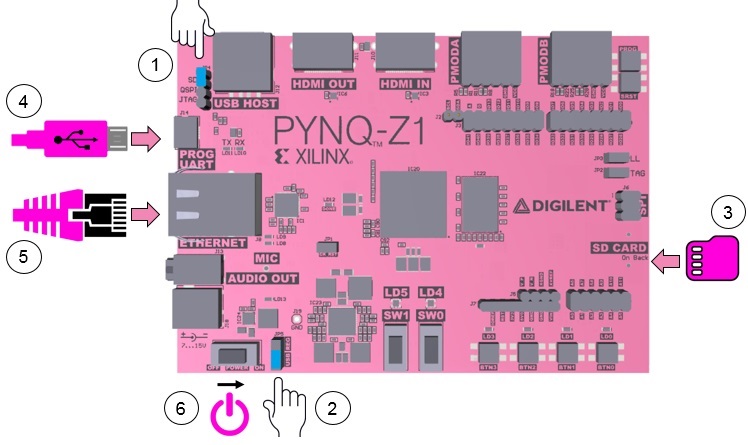 |
|---|
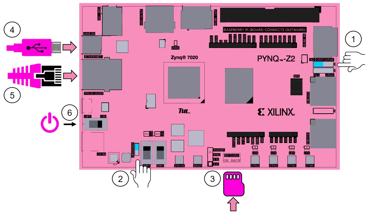 |
| :--: |
| Figure 15. PYNZ-Z1 and PYNZ-Z2 boards |
Follow the steps below:
- Set the JP4 / Boot jumper to the SD position by placing the jumper over the top two pins of JP4. This sets the board to boot from the Micro-SD card.
- To power the PYNQ from the micro USB cable, set the JP5 / Power jumper to the USB position. You can also power the board from an external 12V power regulator by setting the jumper to REG.
- Insert the Micro SD card loaded with the PYNQ image into the Micro SD card slot underneath the board.
- Connect the USB cable to your PC/Laptop, and to the PROG - UART / J14 MicroUSB port on the board.
- Connect the board to Ethernet by following the instructions below.
- Turn on the PYNQ and check the boot sequence (explained below).
Boot sequence:
-
Slide the power switch to the ON position to turn on the board. The Red LD13 LED will come on immediately to confirm that the board has power. After a few seconds, the Yellow/Green LD12 / Done LED will light up (green) to show that the ZYNC device is operational.
-
After a minute you should see two Blue LD4 & LD5 LEDs and four Yellow/Green LD0-LD3 LEDs flash simultaneously. The Blue LD4-LD5 LEDs will then turn on and for some seconds and then turn off while the Yellow/Green LD0-LD3 LEDs remain on. The system is now booted and ready for use.
-
Connect the FPGA board to a computer:
You need a computer with a free Ethernet port [^1]1.
You also need to have the permissions to configure your network interface.
With a direct connection, you are able to use PYNQ.
Follow the steps below to connect directly to a computer using static IP2 address:
- Assign a static IP address (how to).
- Connect the board to your computer’s Ethernet port.
- Open a web browser and browse to
http://192.168.2.99. - The credentials to login on the web page are xilinx/xilinx.
4.2 Running on FPGA
Once logged in, the main screen of the Jupyter notebook is similar to Figure 16. If you are not familiar with Jupyter notebook, you may want to check this tutorial.
 |
|---|
| Figure 16. Jupyter notebook web page |
The content of the folder riscy is shown in Figure 17.
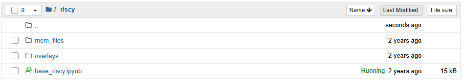 |
|---|
| Figure 17. Folder content |
Inside mem_files you see data.coe and code.coe, which are the memory initialization files for the BRAMs connected to the RISCY core.
The overlays directory contains the following:
base_riscy.bit: Generated bitstream from the main riscy project, can be found inpdp-project/hardware/vivado/riscy/riscy.runs/impl_1/riscv_wrapper.bit.base_riscy.tcl: Generated at the same time as the bitstream, you can find it inpdp-project/hardware/vivado/riscy/riscy.runs/impl_1/riscv_wrapper.tcl.base_riscy.hwh: Hardware handoff file, autogenerated from the riscy project inpdp-project/hardware/vivado/riscy/riscy.gen/sources_1/bd/riscv/hw_handoff/riscv.hwh.
These 3 files will have different names when you generate them using Vivado. Then you should rename them to the same to be able to use them in the Jupyter Notebook and the name should match that of the bitstream when importing it with the Overlay command inside the Jupyter notebook.
You can find a copy of this base directory in pdp-project/hardware/sw/fpga/riscy.
With all the files available and accessible via the browser in the FPGA, you can now proceed to run the base_riscy.ipynb notebook.
This notebook contains the code and explanations to perform the following actions:
- Initialize the notebook, load the overlay (PL image/bitstream) and some helper functions to initialize the BRAMs.
- Program the PL with the bitstream.
- Control the RISCY core by performing AXI writes/reads to the riscv_control module.
- Programming the instruction and data memories.
- Read the instruction and data memories.
- Start/stop the fetching from the core.
- Check the results written by the core to memories or the duration of the test registered by the mem_snoop module.
-
If your laptop has no Ethernet port, you need an Ethernet-to-USB converter. You may ask for it in the weekly meetings. ↩
-
Here, IP refers to Internet Protocol and not Intellectual Property. ↩
First Phase of the project
For the first two weeks of the Processor Design Project (PDP), edition 2025, you are expected to perform the following tasks:
Task 1: Make sure that the basic RISCY core, the LLVM toolchain, and the AES software implementation are all working. Please note that at this first stage, no modifications to the RISCY core or the LLVM compiler are expected. Your job is to synthesize the provided RISCY core including the peripherals and other IPs using Vivado, load the generated bitstream into the FPGA board, compile the base AES software implementation and run it on the RISCY core that was already loaded on the FPGA board. A detailed manual on how to do all of this is provided. Now you are ready to really start the PDP project.
Since in the second phase of the project (starting in week 3) you will be extending this basis RISCY system with the two standard AES encryption instructions AND the loop-unrolling pass for the AES inner round instruction, some additional reading and thinking is expected in the first phase. Moreover, you will be also evaluating and reporting the quantitative improvements provided by your RISCY_AES system against the baseline RISCY + AES in software. In addition, you are expected to propose, implement and evaluate additional system improvement(s). The next tasks will help you with the preparation for the above.
Task 2: Perform a literature review of what has been already done on RISCV, AES hardware implementations and AES specific compiler optimizations. This will familiarise you with the work already done and reported in order to then better decide on the extensions/improvements your team will commit to. Your findings will be described in the background section of your first report (due at the end of week 2). This task will also help you identify the state-of-the-art to compare against your final project results.
Task 3: Analyse the base system bottlenecks (choose your method, e.g., analytical, static dynamic, etc), forecast how the AES instruction extensions and loop unrolling will impact those and make initial plans (hypothesis) how to improve the extended system. The intended improvements can be any of these but not limited to:
- lowest execution latency;
- highest throughput;
- minimal area utilisation;
- minimal memory footprint / register pressure;
- AES specific LLVM optimisation passes for a clear goal;
- (any other quantitative improvement you group commits to work on during the final phase of the project).
Note: Precise energy simulation and measurements can be quite challenging on the FPGA platform used. Please consult the lab sessions team in case you have questions about this. In case you decide to work on LLVM optimisation passes and other extensions, please consult with the TA team.
Task 4: Write your intermediate report incorporating the following. Your hypothesis for RISCY_AES+LLVM extensions, additional improvements and plans on how to implement, debug and validate those. Create a detailed project plan for the second phase (weeks 3 to 8) with internal tasks (do not forget to assign team members to those) and built-in milestones to help with monitor your progress. Please mind that the project has hard deadline at the end of week 8! You are free to decide on the specific internal tasks, their distribution and interdependencies. Please mind that this is a complex project and you are expected to work together as a team. You have to also describe what you will compare against (the state-of-the-art in your background section) and how you plan to obtain the quantitative results needed to support your claims. Do not forget to mention explicitly who contributed what to the sections and activities described in the report.
Deliver your report at the end of week 2 and start with implementing and integrating the AES encryption instructions (aes32esi and aes32esmi). Once this is done, use the LLVM built-in loop-unrolling pass for the AES inner round instruction (aes32esmi). One week later (end of week 3) you will receive detailed feedback in order to improve your original plans for the additional improvements as described in your intermediate report.
Second Phase of the PDP project
In weeks 3 to 8 you will work on two different sets of tasks where the first task is common for all groups.
Task 1
In this task, you will implement standard AES encryption instructions, aes32esi and aes32esmi, in Verilog and integrate with RISCY, known as hardware implementation. On the other side, known as software imeplementation, you modify the software AES code to use the assembly instructions along with the built-in loop-unrolling pass of LLVM for the AES inner round instruction (aes32esmi). You are also expected to evaluate the advantages of the above improvements as compared to the unmodified RISCY core running the AES in software. All of these tasks should be completed before proceeding to the second set of tasks. Briefly, the steps are:
- Implement instructions in Verilog.
- Modify the C code to use
aes32esmiandaes32esi. - Obtain the IR representation of the code and verify that assembly instructions are used properly.
- Apply the LLVM loop-unroll optimization pass to the modified code and verify that the loop has been unrolled.
Please note that hardware and software implementations can be done in parallel by group memebers, however, we recommend you to synchronize yout findings.
The description of the instructions can be found in ZKNE manual. The manual explains how the instructions work and how they should be used. Since the description and general usage of instructions are similar, we only explain the details of the middle round instruction. The format of aes32esmi looks like:
aes32esmi rd, rs1, rs2, bs
Where
- rd: Destination register
- rs1 and rs2: Source registers
- bs: Byte shift value
To be able to use the assembly instruction in the C code, __asm__ directive is used as shown below:
__asm__ volatile (
       "aes32esmi %0, %1, %2, %3"
         : "+r" (X1)
         : "r" (X2),
           "r" (X3),
           "I" (X4)
);
Where %0, %1, %2, and %3 are corresponding to rd, rs1, rs2, and bs, respectively. Please note that you have to complete the instruction by properly filling X1...X4.
To verify that the modified code, you can quickly compile and execute the code and compare the output (encrypted text) with the software implementation code. Since the input and key are hardcoded in the source file, it is expected to get a single unique output.
Once you have verified that the assembly instructions are functionally correct, you can proceed with LLVM optimization passes. Here, we focus on the loop-unroll pass on the initial IR representation, so the effect would be the unrolled middle round of AES encryption. While there are several passes overlapping functions, it is mandatory to apply loop-unroll and get the final correct result. To check if the loop has been unrolled, you should first count the number of aes32esmi instructions inside the original loop and then multiply that by the number of iterations, fixed 9 times. The same number of instructions must be observed in the unrolled version.
Task 2
The second set of tasks is aimed to implement, debug and validate the group specific system improvements. Generally, each group has to propose an idea and hypothesis in the intermediate report. The confirmation and feedback is given TA team. Please note that this part will be completely different for each team as well as the reference baseline for comparison (aka state-of-the-art) that will be used for validating the implemented improvements.
Report Preparation
This course needs two reports. The first is the intermediate report which is due on Friday 2/5/2025 and the second is the final report due on Friday 20/6/2025. We have provided a TEX template which can be used for both intermediate and final reports. Please note that reports must be submitted in PDF format. While both reports share some common structures and chapters, the intermediate report should look like a proposal while the final report should look like a comprehensive report covering all activities that have been done throughout the course.
Notes:
- Please only use the provided template and avoid other templates, e. g. conference like reports.
- For consistency, please use this format for the file name pdp_final_report_group_XX.pdf.
Intermediate Report
The intermediate report is not optional and is delivered per group. It is meant to be a midterm status check and for providing you with feedback on your specific plans for the second phase of the project. Your report should contain the following items:
- Introduction which covers
- Problem Statement: Briefly describe the baseline processor design, outlining its main features, strengths, and weaknesses.
- Motivation: Explain the rationale behind your optimization proposal—what inspired your changes and how you identified opportunities for improvement.
- Background which describes relevant previous works.
- Hypothesis which covers your idea about the proposed RISCY_AES and/or LLVM extensions and other intended improvements. You must answer (at least) these questions: What, How, and Why?
- Plan which covers your plans on how to implement, debug and validate those. Please include
- A detailed project plan (GANTT chart) for the second phase with internal tasks and milestones.
- A plan for the obligatory AES instruction extensions and the loop-unrolling pass of the LLVM at the beginning of the second phase.
- A plan for assigning team members to the tasks.
- Your selection for a baseline to compare against (the state-of-the-art in your background section, or the default implementation are both valid baselines--when comparing to the state-of-the-art you are not necessarily expected to beat the state-of-the-art).
- A plan on how to obtain the quantitative results needed to validate your claims.
- Individual contribution which lists the activities that have been done by each member of the group during the first phase.
Final Report
By the final day of the course, all student groups are required to submit their final report through BrightSpace. The report should be organized into four logically connected chapters, each building upon the previous, with clear transitions between them. The recommended structure is as follows:
- Introduction:
Provide a concise overview of your entire project, addressing the following points:
- Problem Statement: Briefly describe the baseline processor design, outlining its main features, strengths, and weaknesses.
- Motivation: Explain the rationale behind your optimization proposal—what inspired your changes and how you identified opportunities for improvement.
- Implemented Changes: Summarize the specific modifications made to the processor, highlighting their intended effects.
- Main Results: Present the key outcomes and their implications.
- Conclusions: State your principal findings in a few clear points.
- Motivation: Expand upon your initial analysis of the baseline processor, detailing the process you followed to identify its limitations. In this chapter:
- Clearly explain why you selected particular optimization ideas and how you assessed their feasibility.
- Justify your design decisions with reference to expected results and potential trade-offs.
- Provide a comprehensive and descriptive account, going beyond the summary in the introduction.
- Proposed Solution: Present the details of your optimization and the specific changes implemented in your processor design. This section should:
- Use diagrams and figures to illustrate new architectural components or modifications.
- Describe your solution from the top level down, making it easy to understand the overall design and the placement of each new or modified component.
- Emphasize components that require special implementation or unique approaches.
- Experimental Results: Report and analyze the outcomes of your modifications. For this chapter:
- Present experimental results separately for each individual modification, as well as for combinations of improvements.
- Compare the performance and resource costs of your enhanced design against the baseline and between different optimizations.
- Include detailed results such as timing information, critical path analysis, resource utilization (e.g., from Vivado reports), and power consumption figures for all relevant designs.
- Discuss key performance metrics, such as area (A), critical path delay (D), energy consumption (E), and any combined metrics you find meaningful.
- Comment on the impact of each improvement, identifying which changes contributed most significantly to each performance metric.
- Conclusion: Summarize your work, main findings, and propose possible directions for future development. In your conclusion, address:
- The initial plan and objectives.
- Your expectations at the outset.
- The actual results obtained, with reflections on any discrepancies between expectations and outcomes.
Supplementary Material
All supplementary materials, such as source code and scripts, must also be included and made available to facilitate further evaluation.
Additional Recommendations
Please take the following tips into account when preparing report files.
- General Structure
- Title Page: Include the project title, group members’ names and IDs, course name, instructor, and date of submission.
- Table of Contents: Helps the reader quickly navigate the document, especially if it is long.
- List of Figures and Tables: Optional, but useful if your report contains many diagrams and tables.
- Within Each Chapter
- Clear Section Headings: Use numbered headings and subheadings (e.g., 2.1, 2.2) for organization and clarity.
- References: If you rely on any external sources, literature, or textbooks, include a references section at the end. Cite any tools (e.g., Vivado) and relevant documentation.
- Appendices: Place detailed design files, long code listings, or extra data in appendices to keep the main report focused and readable. Refer to them in the main text as needed.
- Specific Content Suggestions (in an Appendix)
- Team Contributions: Briefly outline the contribution of each group member. This promotes transparency and it is required by the instructors.
- Version Control: If you used a version control system (e.g., Git), mention this and summarize your workflow or any challenges encountered.
- Design Challenges and Solutions: Consider adding a section or short paragraph reflecting on major obstacles faced during the project and how you overcame them.
- Lessons Learned: Share key takeaways from the project—both technical and collaborative—which could be helpful for future students.
- Presentation
- Professional Formatting: Ensure consistency in fonts, spacing, and citation style. Number pages.
- Clarity and Brevity: Aim for concise, clear writing. Use bullet points and tables where appropriate to present information efficiently.
- Figure Quality: Use high-resolution diagrams and ensure all figures are clearly labeled and referenced in the text.
- Final Checklist (Essential!)
- Proofread the report for typos, clarity, and logical flow.
- Double-check that all required results and analyses are included.
- Ensure all files (PDF report, any required code, design files, etc.) are present in the zip archive.
- Recommended Report Length
- Main Report: Around 18–20 pages. This includes the Introduction, Motivation, Proposed Solution, Experimental Results, and Conclusion.
- Appendices: Unlimited (as needed) which are used for:
- Extensive Vivado reports
- Large tables of raw data
- Detailed code listings
- Supplementary diagrams
- Front Matter (Title page, ToC, etc.): Not counted in the main page range above.
- Breakdown by Section (as a guideline)
- Introduction: 1–3 pages
- Motivation: 2–4 pages
- Proposed Solution: 3–6 pages (more if complex, with figures/diagrams)
- Experimental Results: 4–7 pages (including tables and discussion)
- Conclusion: 1 page
- Tips:
- Focus on clarity and depth rather than just length.
- Use diagrams and tables to communicate efficiently.
- Do not pad sections unnecessarily—concise, well-explained points are better.
In this section we describe in detail how this course is graded. First, there is a group grade based on
- Whether the intermediate report was submitted and phase one was completed or not.
- Technical merit of the work done in phase two as described in the final report.
- Quality of the final report.
Second, after determining the group grade, the grades will be individualized via a peer review process among the members of the group.
Group Grade
The final group grade is calculated by adding the achieved points of the three items below:
Fundamental (3 points)
This consists of the Intermediate Report (IR) plus Phase One. Every group should have completed both during the quarter. This part is considered as all or nothing meaning that the group gets either 0 (nothing) or 3 (all).
Technical Merit (5 points)
This consists of the average of the two grade items below:
-
Proposed/Implemented Solution (0 to 5)
- 0 (fail) - unsystematic approach, no validated use of research/design methodologies, no explanations, nothing beyond phase one
- 1 (sufficient) - partial/incomplete analysis and motivation of one solution only, no trade-offs discussion
- 2 (satisfactory) - shallow analysis and motivation of one solution, e.g., only focusing on hardware or software, limited trade-offs discussion
- 3 (good) - shallow analysis and motivation of multiple solutions in either or both hardware and software, some trade-offs discussed
- 4 (very good) - in-depth analysis and motivation of proposed solution in hardware or software, trade-offs explained
- 5 (excellent) - in-depth analysis and motivation of proposed solution in hardware and software, trade-offs well-explained, work could potentially be published
-
Interpretation of Results (0 to 5)
- 0 (fail) - insufficient interpretation and no verification of results, no comparisons at all, no or some (unrelated) conclusions are drawn
- 1 (sufficient) - findings are treated as straightforward and unproblematic, minimal verification, incomplete comparisons, conclusion are sufficiently linked to results
- 2 (satisfactory) - findings are treated as straightforward and unproblematic, some comparisons, verification was carried out, conclusions are based on results
- 3 (good) - uses techniques for interpretation and verification in a mechanical way, mechanical comparisons without discussion, conclusions based on results in a clear way
- 4 (very good) - good interpretation and verification, detailed comparisons with chosen baseline or related work, conclusions are based on results in a clear way
- 5 (excellent) - detailed interpretation and verification of results, detailed comparison with chosen baseline and related work, conclusions are based on results in a clear way and are extrapolated to a wider context
Quality of Report (2 points)
This can be either
- 2p which means the report follows the template completely.
- 1p which means the report follows the template partially.
- 0p which means the report does not follow the template at all.
Peer Review
This part is done by the group members. Every student will be asked to assign values to their colleagues’ performance based on the following criterias to answer "how did my colleagues perform within the group?"
- Effort (0-5) - How much did student contribute to the group?
- Presence (0-5) - Availability during meeting, reachability, communicativeness
- Dependability (0-5) - Responsibility to group, trustworthiness, seriousness
- Quality of work (0-5) - Compatibility of work, interfacing with other works
- Overall contribution (0-5)
Procedure and Example
Figure below shows the procedure along with an example on how the course grade is calculated based on the group grade and individual contribution. Please note that in the peer review, each member receives a grade from his/her colleagues. That grade is compared against a benchmark average which shows the student's score compared to the average. The value shown in this figure is just an example and the final value may change by the instructors.

# Frequently Asked Questions
Can somebody take a look at my design? I have some errors that I do not manage to solve.
No, we cannot debug your Verilog and LLVM code for you. There are weekly lab sessions in which you can ask questions about technical issues you're facing. However, we generally expect you to debug your own code. We highly recommend using version control software to keep track of old versions of the code by each team member such that you can go back to a working version.
Can I have a discussion with you about the design? I have some ideas to improve it.
Yes. There are weekly labs in which those things can be discussed. Prior and after those, you may email your questions to CESE4040.2025@tudelft.nl.
Can I install the toolchain on my own laptop?
Yes, but we do not recommend that. All software tools have been installed on the server to mitigate installation and configuration problems. If you have a problem working with the server, please inform the TA team to fix the issue. Installing the toolchain locally on your laptop takes time and you may not be able to reach the deadlines. Additionally, you may miss specific versions of the toolchains that are setup on the server. If you decide to install the softwares locally, the TA team will not be able to assist you with configuration and installation errors.
When a group member accesses the remote desktop on the server, other members are not able to access the desktop. How is that solved?
With X2Go it is possible to have different remote desktop views with a single user name. Please read this page on how to have multiple sessions on the server.
X2GO client on Linux often crashes. What can I do?
We recommend using X2GO client on Windows host as it is more stable than Linux host.
Should each group set up an access token on the Gitlab website?
No. We recommend each member of the group to create a folder with his/her name and clone the repository with his/her personal access token for further modifications. The member is then able to commit and push to the group repository.
When I want to synthesise the project with Vivado on the server, I get the "time-out" error or the screen freezes for a long time. What should I do?
Please note that due to the resource limits and high number of simultaneous jobs, it might be possible that the server becomes overloaded. While we do our best to ensure that enough resources are available to groups, we recommend rerunning the job later on to contact the TA team if the problem persists.