3. PDP Project
3.1 Vivado
To launch the Vivado Software, open a terminal and type vivado. For your convenience, several scripts are provided with the base RISCY repository mentioned earlier. These scripts can be executed directly from the Vivado’s TCL console. To do so, first change your directory to pdp-project/hardware/ then use source command as shown Figure 6.
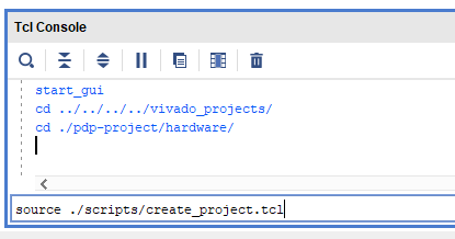 |
|---|
| Figure 6. TCL Console |
Alternatively, you can execute the script by invoking vivado command vivado -mode batch -source <your_Tcl_script> with the same effect as Figure 6.
3.1.1 Project Creation
A dedicated script to generate the base FPGA system that will be used for simulation and implementation. The script is located at pdp-project/hardware/scripts/create_project.tcl. After running this script, your project is loaded in Vivado as shown in Figure 7.
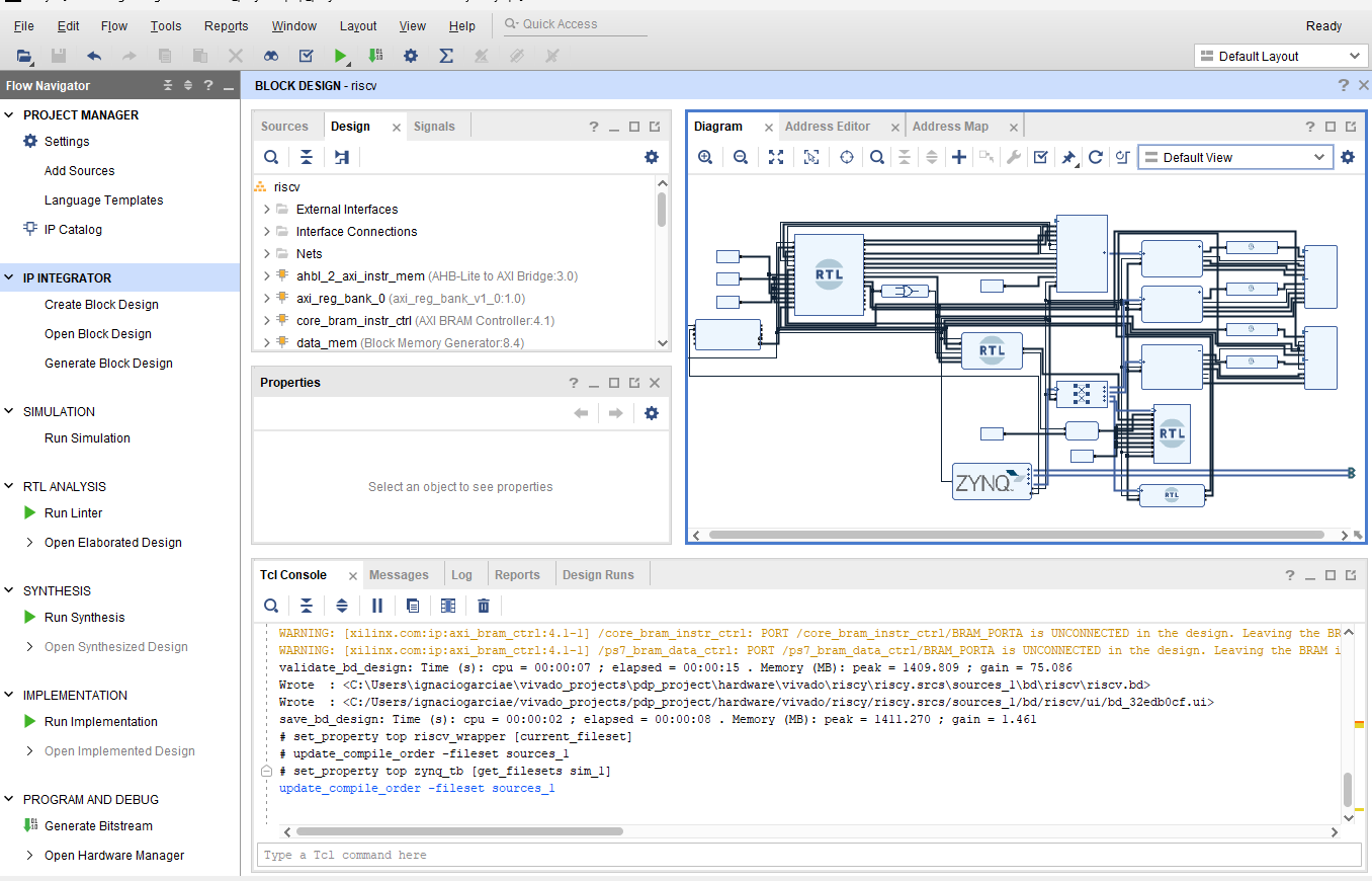 |
|---|
| Figure 7. Loaded project in Vivado |
Under the Sources tab, you can find both the RTL source files, constraints and simulation sources, as shown in Figure 8. Selected top levels, often referred to as tops, are shown in bold font. There are two tops in every design, one for the Design Sources, used for synthesis and implementation, and one for the Simulation Sources, used for simulation. More information is provided next.
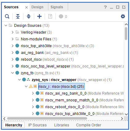
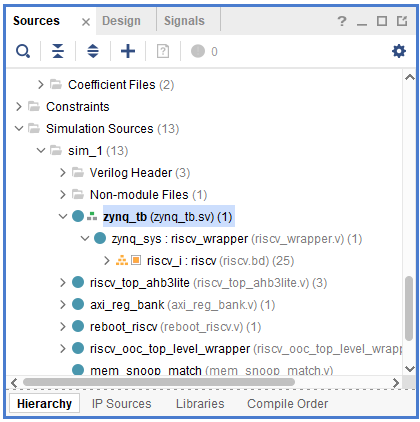
Figure 8. Sources tab
3.1.2 Top Level Design
The design top level source is a block diagram autogenerated using one of the provided TCL scripts in pdp-project/hardware/scripts/generate_fpga_bd.tcl and is shown in Figure 9.
 |
|---|
| Figure 9. Block diagram of the design |
This block diagram shows what will be synthesized and loaded on the FPGA. It consists of the following relevant blocks/modules:
riscv_top_ahb3lite: Wrapper around the top level of RISCY, it includes the interfacing IPs1 used to connect the core to on-chip FPGA SRAM memory blocks, also referred to as BRAMs.instr_mem: Dual port BRAM containing the instructions executed by your processor.data_mem: Dual port BRAM containing the data.procesing_system7: Instance of the hardened ARM core available in the FPGA device, used to generate the clock of your processor design and to write/read data to and from the other IPs, e.g. program and data memories, of the design via an AXI bus.mem_snoop_match: Small module in charge of snooping the data memory interface, configured to spot the end sequence,0xDEADBEEF, at address0x2000. Also counts the clock cycles since its clock enable input is asserted (connected to fetch enable) until the end sequence is found.reboot_riscv: Control block used in the design to assert/deassert the fetch enable and reboot signals connected to the core.axi_reg_bank: Register bank used to be able to access PL2 signals via AXI from the processing system.- Interconection blocks:
Smartconnect(used to access from a single processing system AXI master three AXI slaves), bram controllers and AHB3-Lite to AXI adaptor (needed to interface between different protocols used by Vivado IPs or the core and the native BRAM interface), and so on. shift_addr: Used given that the generated BRAMs by vivado are addressed per word, instead of per byte as AXI and our core do. Since the word width of the BRAMs is 4-bytes, we just shift the input address by 2 bits.
3.1.3 Top Level Simulation
System simulation:
The testbench source file can be found at pdp-project/hardware/src/simulation/zynq_tb.sv.
The testbench just generates the necessary clock and reset signals, connects them to the top level of the design, and performs some reads/writes via the processing_system AXI.
Both instructions and initial data are preloaded into the BRAMs by the generate_fpga_bd.tcl script, where you can check that the memory initialization files being loaded are code.coe and data.coe and should be placed in pdp-project/hardware/src/sw/mem_files.
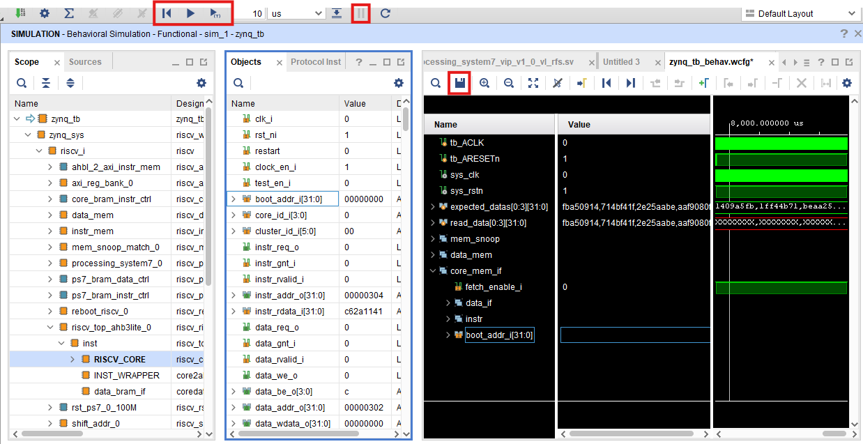
A script has been provided to run the simulations and preload a selection of waveforms. To use it just run source ./scripts/run_simulation.tcl. It will take around a minute to elaborate all the project sources and then it will run the simulation. Depending on the code being executed in the core it will take more or less than four minutes to simulate the baseline software AES encryption. Once the simulation finishes your Vivado window will look like Figure 10.
 |
|---|
| Figure 10. Simulation output |
The waveform window with the preselected signals is highlighted in red. You can always add or modify the selected signals and save your view. This way the next time you run a simulation with the script it will show your own version.
If you add signals that were not selected before running the simulation, you will only be able to see their final value. Click on Restart, and then on Run as shown in Figure 11.
 |
|---|
| Figure 11. Waveform output |
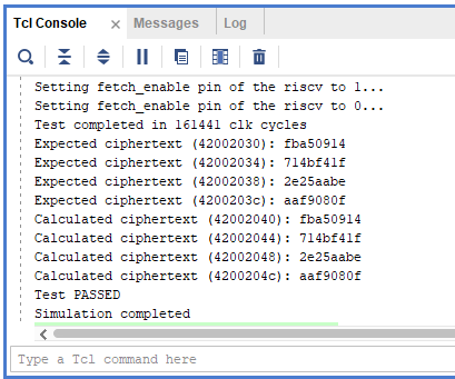
You can always stop the simulation at whatever point you want by using the Pause button. The console output of the base project by the end of the simulation is shown in Figure 12.
 |
|---|
| Figure 12. Console output after simulation finishes |
Module simulation:
Only testbench files and scripts for system level simulation are provided (core + memories), if lower-level testing is required (i.e: modules that are part of the core) you are expected to implement all of the required files (testbench, testcases, scripts) needed to verify and debug your project yourself.
3.1.4 Synthesis and Implementation
If you just want to verify your changes to the RISCY core or how does the resource utilization changed, it is recommended to just run an OOC3 synthesis as it will be faster than running synthesis on the entire project.
To run the OOC synthesis just open a new vivado window, change directory to the hardware directory and then source this script pdp-project/hardware/scripts/create_project_ooc_synth.tcl. This script will also save the results in pdp-project/hardware/vivado/ooc_riscy/ooc_riscy.runs/ooc_synth/. In Vivado the reports look like Figure 13.
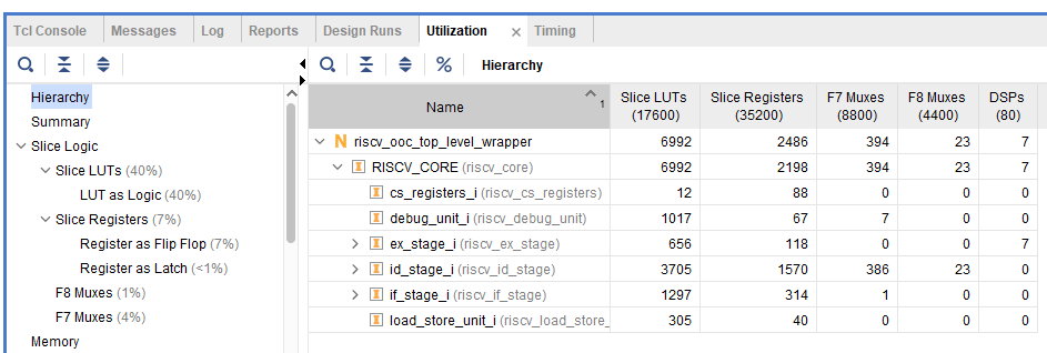
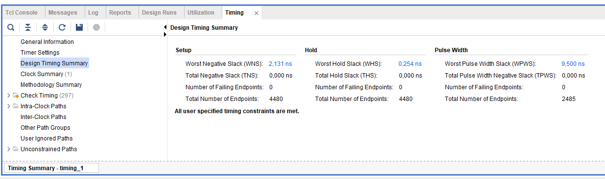
Figure 13. Timing and utilization reports
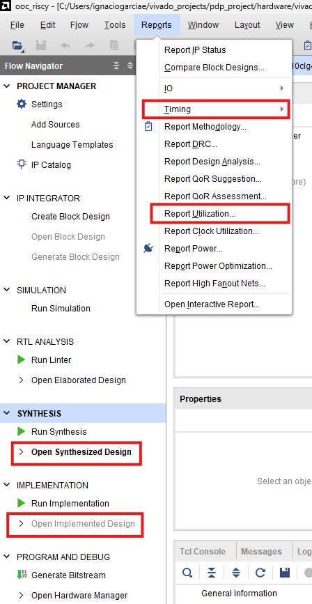
To generate these reports manually for any design, just click on Open Synthesized Design or Open Implemented Design depending on the step you got and then on Reports->Timing or Reports->Report Utilization for Utilization/Timing as shown in Figure 14.
 |
|---|
| Figure 14. Reports menu |
If you want to run synthesis or implementation for the full project manually, you can always use the Run Synthesis or Run Implementation options.
3.1.5 Bitstream Generation
You can generate the FPGA bitstream from your RISCY project by just sourcing pdp-project/hardware/scripts/run_synth_impl.tcl. You can also create the project and generate the bitstream with a single script by sourcing pdp-project/hardware/scripts/gen_bitstream.tcl from a new vivado window. You can find the generated bitstream at pdp-project/hardware/vivado/riscy/riscy.runs/impl_1/riscv_wrapper.bit.
Note: It is always advised to generate timing and utilization resources of the implemented design before trying to use the bitstream on the board, this way you can spot any possible timing violations or RTL getting optimized away.
3.2 Application: AES Code (C)
The baseline software implementation of the AES encryption is provided in C and can be found in pdp-project/software/main.c.
This source file contains all the functions used to perform the encryption, the initial text, the key to be used and the expected ciphertext. For example, the input text “Hello, World!000” and the key “cese4040password” are hardcoded in the program.
The main function of this C file just performs the encryption of the input text, writes the ciphertext and the expected ciphertext to a given address, checks the output and writes either 0xBAAAAAAD or 0xCADEBABE depending on if the ciphertext matches expected, and writes the end sequence 0xDEADBEEF detected by the mem_snoop module on the FPGA to a specific address 0x0102000.
Note: The ending sequence should not be removed, as it is used by the testbench to know when the core finishes with the execution of the main and stop the simulation.
3.2.1 Compilation and Setup
It is first necessary to update the paths within the pdp-project/software/config/rv32-standard.conf to point to the specific directories where the RISC-V GCC toolchain and LLVM are located.
To do this modify, if needed, the paths assigned to the variables RISCV_GCC and LLVM.
To compile the C code and generate the executable binary, and also the memory initialization files used by the FPGA project, it is only needed to run make soft within the pdp-project/software directory. This will create the binary in pdp-project/software/output/soft.elf and the memory initialization files (.coe) files in pdp-project/software/bin_files.
These generated .coe files need to be copied to the FPGA project, pdp-project/hardware/src/sw/mem_files, so they can be picked up by the simulation flow.
-
Intelectual Property (IP). ↩
-
Programmable Logic (PL). ↩
-
Out Of Context (OOC) Synthesis is a technique used in FPGA design flows, where individual modules or IP blocks are synthesized separately from the top-level design. This is helpful when performing sanity checks to the RISCY core is required without synthesizing the whole FPGA design. ↩