Lab 1
In this lab, you will be putting your Verilog skills to practice. You will write hardware descriptions for different applications and synthesize and implement these designs using Xilinx Vivado. Then, after synthesis and implementation, you will generate a bitstream of your design to upload to an FPGA board. On the FPGA board, you will test your designs.
During the lab, you will be using Vivado software. You need to install it before the lab. Installation instructions are available in Vivado Setup If you cannot not install Vivado, talk to one of the TA's and follow the instructions in Backup option to use the lab server.
If you are new to Verilog or Hardware description languages, it is recommended that you go through the Verilog Tutorial before the lab. This will help you understand the workflow of how a hardware description program is written and the main building blocks of a Verilog code.
Table of Content
- Part 1: Asynchronous Encoder & Decoder
- Part 2: Debouncing of electrical signals
- Part 3: Finite State Machine (FSM)
- BONUS: Linear Feedback Shift Register Random Number Generator
Download the Vivado project templates used in this exercise here: Vivado_Lab1
Part 1: Asynchronous Encoder & Decoder
In this lab, you will use a binary rotary switch and a gray code rotary switch to perform some basic asynchronous decoders.
Learning Goals of the Lab
- Introduction to Vivado and Vivado toolchain
- Understanding block diagrams, inputs, and outputs of the FPGA
- Implementing Asynchronous logic
Lab Template:
For all the exercises in this lab, you will receive a basic template for you to work on, except the bonus exercise. For this lab, we describe the components in the template. From the next exercises, you are expected to explore the template on your own.
To start the lab, launch the Vivado application. Open the project Async_Encoder_Decoder in Vivado. It will open the following screen.
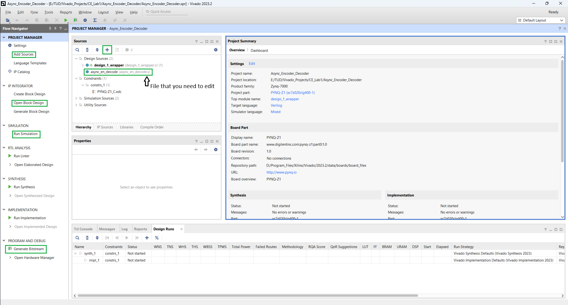
Above you can see the file async_en_decode.v, which needs to be edited to complete the assignment. Other functions that you will be using in the lab are also highlighted.
You can now Open the Block Diagram. A block diagram is a visual representation of all the interconnected IPs and Verilog blocks with each other and with external components. The block diagram for this project is shown below.
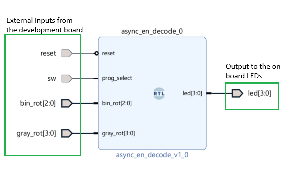
There are 3 main parts to the above block diagram.
- Inputs coming into the block diagram from the board. These include:
- Reset switch: Mapped to SW1
- SW switch: Mapped to SW0
- Binary Rotary Encoder: Mapped to PMODB[0:2]
- Gray Encoder Switch: Mapped to PMOD[4:7]
- In the middle is the RTL code you will write in the Verilog file.
- Finally, the output LEDs are mapped to the on-board LEDs
The above-mentioned component mapping is done in the constraints file. This file is located in Sources -> Constraints -> constrs_1 -> PYMQ-Z1_C.xdc. You can open and explore how the physical pins on the FPGA are mapped to various external components. These files are different for every development board, based on the on-board components.
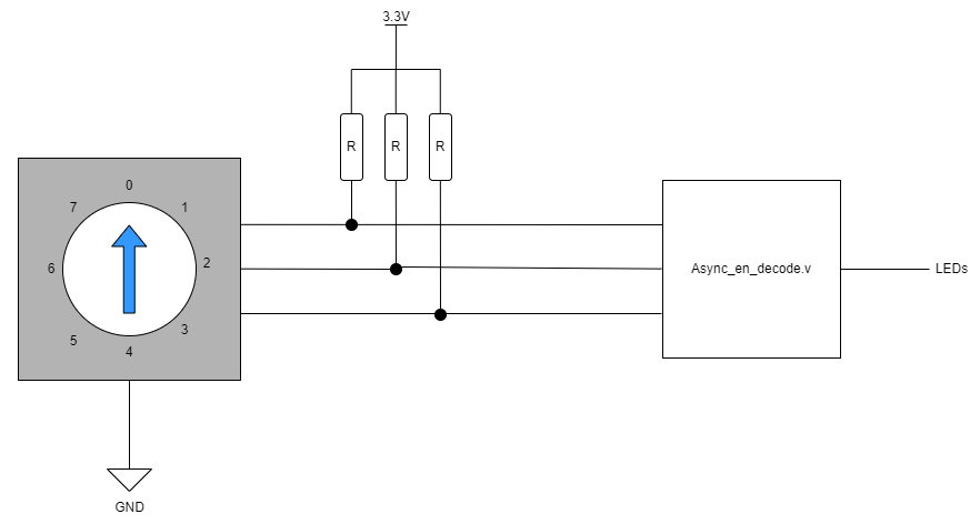
Step 1: Binary Display
Now that you are a bit more familiar with the Vivado tool. Open the async_en_decode.v file. In this exercise, you will be mapping the binary input from the binary rotary switch to the on-board LEDs.
Follow the following steps to complete the assignment:
- Make an asynchronous
always@(*)block in the module - Implement the reset switch logic:
- If the
resetsignal is on, your code should turn off all the LEDs - Only if
resetis off, the rest of the code should be executed
- If the
- Map the
bin_rotinput to theled[2:0]output. Refer to the circuit diagram below.- Note: The rotary switch is connected with pull-up logic
- Make a testbench for your project and simulate.
- You can find the steps to making your testbench in Simulation & Synthesis
- Once you have the testbench working as expected you can move on to Step 2
The data sheet for the binary rotary switch being used: Binary Rotary Switch (S-8010)
Step 2: Cardinal Direction Decoder
In this exercise, you will interface with the gray rotary switch and convert the inputs from the gray rotary switch into Cardinal directions.
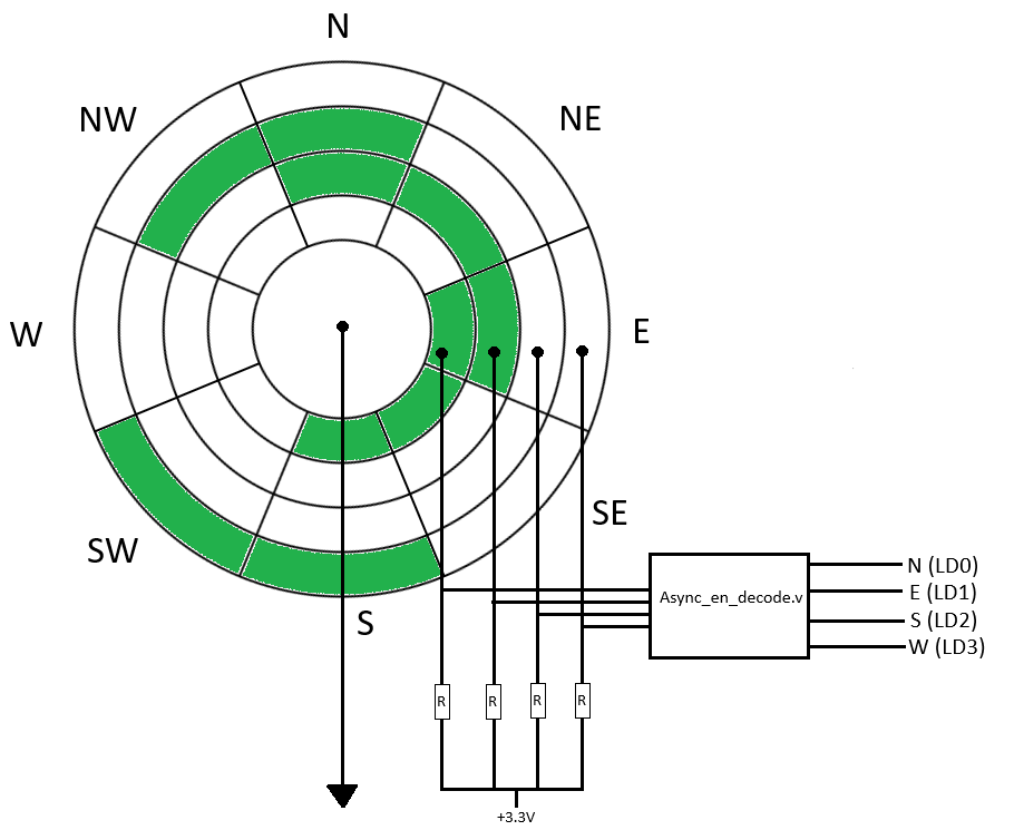
As you can see from the above image, you have to translate the rotary switch output into cardinal directions. For example, if the wheel is in the North position, only LD0 should be on and if the wheel is in the South-West direction, then both LD2 and LD3 should be on.
Follow the following steps to complete the assignment:
- Since you are going to use the same project for 2 programs, you need to use the
prog_selectswitch- When the switch is
UPthe binary display from Step 1 should be executed - When the switch is
DOWNthe Cardinal Direction Decoder should be executed
- When the switch is
- Implement cardinal direction decoder logic in
async_en_decode.v - Modify the testbench to test cardinal direction decoder logic
- Once successfully tested, generate bitstream, and program the FPGA to test binary display
- Call a TA to test your final design and test your cardinal direction decoder on hardware
The data-sheet for the gray rotary switch being used: Grey Rotary Switch
Part 2: Debouncing of electrical signals
In this lab, you will work with the on-board buttons and make a binary and gray-encoded counter.
Learning Goals of the Lab
- Interface with buttons on the board
- Use Debouncing and understand its need
- Implement synchronous logic
- Programming and testing the FPGA
Step 1: Binary Counter
In this step, you should implement a synchronous binary counter, and display the value using the on-board LEDs. When BTN0 is pressed, the counter should increment, and BTN1 is pressed the counter should decrement.
Note: Do not forget to implement the reset logic, similar to Part 1
- Open the
Debouncerproject in Vivado - Implement synchronous logic to increment and decrement the counter and display it on the LEDs
- DO NOT modify the block diagram yet
- Write a testbench for the module and simulate it using the simulation tool in Vivado
- Generate bitstream and upload it to the FPGA
Did the counter work as expected? Read more about what is debouncing and why do we need it: Debouncing
Step 2: Adding Debouncing
Here, we introduce debouncing logic in our project. This should remove all issues with your program getting multiple button presses.
- Open the Block-Diagram
- Disconnect the encoder
A&Binputs from the buttons - Connect the inputs to the
btn_outof the debouncer block - Simulate to verify that you have made the connections correctly
- Generate the bitstream and program the FPGA
Step 3: Converting to Gray Encoding
In this step, you will convert your binary value into a gray encoded value and display it on the LEDs
- Add an additional asynchronous block to convert the binary value into a gray encoded value
- Use an internal register to store your binary value
- You can use a look-up table for the conversion or use the gray encoding equations for 4-bit numbers
- Simulate to verify that you have made the encoding correctly
- Generate the bitstream and program the FPGA
Note: You can refer to Gray Encoding.
Once completed, please call the TAs who will approve your work and you can continue with the rest of the lab.
Part 3: Finite State Machine (FSM)
In this part, you will be implementing an FSM for a Road Safety Sign. The particular sign that you need to implement has the following modes:
- Arrow Point Left
- Arrow Point Right
- Blinking Lights Warning Mode
- Safe Mode
Learning Goals of the Lab
- Understanding and Implementing a Finite state machine
- Understanding different components and types of FSMs
To complete this exercise, use the Road_Sign provided in the template folder. Open it using Vivado. You will need to modify Road_Sign\Road_Sign.srcs\sources_1\new\road_sign.v to implement the encoder.
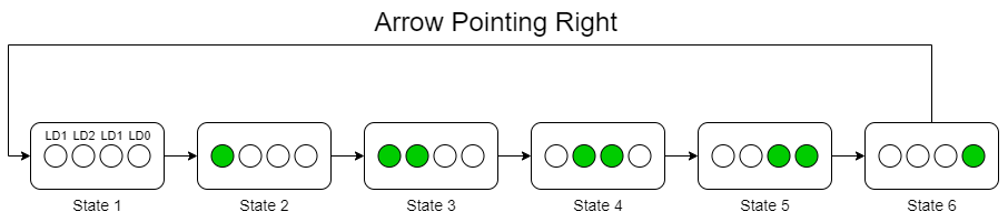
Step 1: Circular FSM
First, you will implement only the Arrow Pointing Left Mode. In this mode, the LEDs light up in a sequence moving towards the left. This is used to let the people know to divert to the left side of the road.
Since we have only 4 LEDs on the board, a pattern of running left LEDs is used to point left. For this, you will implement a 6-state circular FSM that has the following states:
![]()
For the FSM to switch between the states, we have a time constraint. Every state transition should take place after 500ms. To achieve this, you can use the provided clock which is of 125MHz, and divide it appropriately so that the state update happens when expected.
Step 2: High-Level FSM
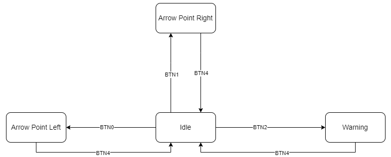
Once you have Point Left working correctly, you need to implement a higher-level FSM to control which mode the Road Sign is in.
To complete this step follow the following steps:
- Make an independent 4-state FSM
- The 4 states are Point-Left; Point-Right; Warning; Idle
- The FSM state change is triggered by the 4 on-board buttons. When the corresponding button is pressed the FSM should enter that mode
- Point-Left: BTN0
- Point-Right: BTN1
- Warning: BTN2
- Idle: BTN3
- Before implementing the functionality of these states, verify that the high-level FSM is working as expected
- Use the RGB_LED1 to verify your functionality (Map 1 color to each state)
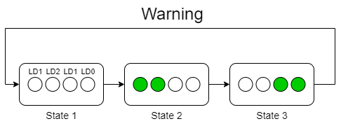
- Duplicate the circular FSM used before and use it for Arrow Point-Right and Warning. As shown in the below figures
- In the Idle state ensure that all the LEDs are turned
OFF.
Step 3: Introducing Safe State of Execution
In the High-Level FSM implemented in the last step, any state can enter any other state. Which is a very unsafe way to transition between states. Since the road sign is deployed in a hazardous outdoor environment like a road-work site, it is important to have an additional safety measure. This can prevent accidental changes in the state of the sign, which can be hazardous on an active highway for example.
Thus, you need to add a constraint to the high-level FSM. You need to ensure, that if the FSM is in Point-Left, Point-Right, or Warning State it can only go to Idle state. And when in the Idle state it can enter any other state. A basic FSM diagram is presented below:
BONUS: Linear Feedback Shift Register Random Number Generator
What are LFSRs:
Linear Feedback Shift Register(LFSR) is a commonly used method to generate a set of pseudo-random numbers since it theoretically will be able to cover all the possible inputs for any n-bit circuits. A schematic of a typical LFSR is demonstrated in the figure below. A characteristic polynomial demonstrates the representation of the structure of the LFSR.
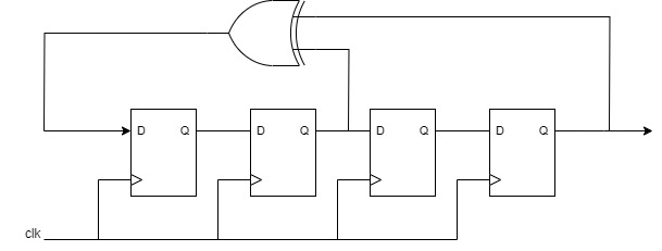
In this example, the characteristic polynomial is \(P(x)=x^4+x^2+1\), which indicates that the first bit will be the XOR result of the 4th and 2nd bit. Repetition distance stands for the number of cycles that the two same generated pseudo-random numbers appear twice. To get the cycle counter, you will implement an internal counter to record the cycle. Seed it as the initial value of the internal register after you press the "reset" button.
Lab Procedure
Implement a 6-bit LFSR with the polynomial of \(P(x)=x^6+x^5+x^3+1\), with three seeds, different seeds.
| Seeds Stored |
|---|
| 6'b00_0000 |
| 6'b01_1001 |
| 6'b10_1001 |
Follow the steps below to complete this lab:
- Open Vivado and make a new project (no template is provided for this part)
- Instructions on making a new Vivado project can be found in Vivado Project Setup.
- Implement a LFSR logic with the polynomial \(P(x)=x^6+x^5+x^3+1\) in the project
- Add logic to check when the LFSR loops back and starts repeating the sequence
- We recommend having a repetition signal as an output, it can go high when the LFSR value is the same as the seed value
- Write a testbench to test the LFSR Implementation
- Simulate the LFSR using the 3 seeds mentioned above
- Record the repetition distances for all three seeds
Once you have finished the simulation, please call a TA for implementation verification.