Computer Engineering
This is the homepage for the computer engineering course. You can find all course information here.
This course is part of the CESE masters programme. This course's curriculum will be continued by the course Processor Design Project
Course Description
The goal of this course is to explain in significant depth what is involved in designing a computer system and to provide more detailed knowledge on specific topics in the area of Computer and Embedded Systems Engineering. The course introduces the entire computer engineering stack and it’s interconnecting layers consisting of both hardware and software. Along with the main principles behind design tools and techniques used in this field. This makes the course an excellent introduction to the field of Computer and Embedded Systems Engineering, the widely used terminology and the most relevant current trends.
Learning Objectives
By the end of the course you will be able to:
- Describe number representation system, conversion between number representation.
- Perform binary arithmetic operation such as addition, multiplication, and division.
- Implement fixed- and floating-point numbers in C/C++ and compare their accuracy.
- Explain basic concepts of computer architecture such as processing unit, memory system, control unit and datapath.
- Use logic gates to implement simple combinational circuits such as adder, multiplexer.
- Write a simplified RISC-V assembly code and Cuda program for grayscale image conversion.
- Explain system software and operating systems fundamentals, task management, synchronization, compilation, and interpretation.
- Use design and automation tools to perform synthesis and optimization.
Course Schedule
Lecture Schedule
| Topic | Date & Time | Location | |
|---|---|---|---|
| L1.1 | Representing Numbers | 4th Sept (13:45) | EEMCS-Hall Ampere |
| L1.2 | Binary Computer Arithmetic | 6th Sept (08:45) | AS-Hall E |
| L2.1 | Putting together a Micro-architecture, RISC-V | 11th Sept (13:45) | EEMCS-Hall Ampere |
| L2.2 | The Architecture of RISC-V (1) | 13th Sept (08:45) | AS-Hall E |
| L3.1 | The Architecture of RISC-V (2) | 18th Sept (13:45) | EEMCS-Hall Ampere |
| L3.2 | The Role of the Assembly Language RISC-V | 20th Sept (08:45) | AS- Hall E |
| L4.1 | RISC-V Input/Output (I/O) and Interrupts | 25th Sept (13:45) | EEMCS-Hall Ampere |
| L4.2 | Computer Systems Memory Hierarchy | 27th Sept (08:45) | AS-Hall E |
| L5.1 | Processors Working Together | 2nd Oct (13:45) | EEMCS-Hall Ampere |
| L5.2 | Moving the Data | 4th Oct (08:45) | AS-Hall E |
| L6.1 | Scaling out the systems | 9th Oct (13:45) | EEMCS-Hall Ampere |
| L6.2 | System Software and OS | 11th Oct (08:45) | AS-Hall E |
| L7.1 | Compilation and Interpretation | 16th Oct (13:45) | EEMCS-Hall Ampere |
| L7.2 | Design Automation Methods (1) | 18th Oct (08:45) | AS-Hall E |
| L8.1 | Design Automation Methods (2) | 23th Oct (13:45) | EEMCS-Hall Ampere |
| L8.2 | High Level Synthesis (HLS) and Domain Specific methods | 25th Oct (08:45) | AS-Hall E |
Exam: 28th Oct, Monday (09:00)
Lab Schedule
| Topic | Date | |
|---|---|---|
| Lab1 | Numerics &Functional Units | 17th Sept |
| Lab2 | RISCV | 1st Oct |
| Lab3 | Parallel Programing with CUDA | 15th Oct |
| Lab4 | EDA Tools | 22th Oct |
Grading
The course consists out of a written exam and 4 lab assignments, 1 per lab session. Each lab assignment is Pass/Fail and you are required to pass each lab in order to pass the course. The lab should be completed during the lab session, a Pass/Fail will be awarded during the lab session
Passing in all the labs and a final grade of 6 is needed to pass the course.
Staff
The lectures for this course will be given by:
- Motta Taouil
- Georgi Gaydadjiev
During the labs you will interact with the TA team:
- Ismael
- Konstantinos
Contact
If you have doubts about the theory part of the course, you can contact Anteneh at A.B.Gebregiorgis@tudelft.nl or Georgi at G.N.Gaydadjiev@tudelft.nl.
If you need to contact the TAs regarding labs, you can find us at the course email address: CESE4130.2024@tudelft.nl.
Alternatively, if you REALLY need to speak to one of the TAs directly, you can contact Himanshu at H.Savargaonkar@student.tudelft.nl or Andre at a.l.herreragama@student.tudelft.nl.
Note that we prefer that you use the course email address.
Slides
Lecture Slides
The lecture slides for the course are on Brightspace.
WEEK-1
- Introduction
- Lecture 1.1
- Behrooz Parhami's Lecture Slides from UCSB
- Behrooz Parhami's Lecture Recordings
- Lecture 1.2
...
- Lecture 8: Slide set 9 and Slide set 10
- Lecture 9: Slide set 11.
Labs
Please note all the labs are mandatory
Lab 1
In this lab, you will be putting your Verilog skills to practice. You will write hardware descriptions for different applications and synthesize and implement these designs using Xilinx Vivado. Then, after synthesis and implementation, you will generate a bitstream of your design to upload to an FPGA board. On the FPGA board, you will test your designs.
During the lab, you will be using Vivado software. You need to install it before the lab. Installation instructions are available in Vivado Setup If you cannot not install Vivado, talk to one of the TA's and follow the instructions in Backup option to use the lab server.
If you are new to Verilog or Hardware description languages, it is recommended that you go through the Verilog Tutorial before the lab. This will help you understand the workflow of how a hardware description program is written and the main building blocks of a Verilog code.
Table of Content
- Part 1: Asynchronous Encoder & Decoder
- Part 2: Debouncing of electrical signals
- Part 3: Finite State Machine (FSM)
- BONUS: Linear Feedback Shift Register Random Number Generator
Download the Vivado project templates used in this exercise here: Vivado_Lab1
Part 1: Asynchronous Encoder & Decoder
In this lab, you will use a binary rotary switch and a gray code rotary switch to perform some basic asynchronous decoders.
Learning Goals of the Lab
- Introduction to Vivado and Vivado toolchain
- Understanding block diagrams, inputs, and outputs of the FPGA
- Implementing Asynchronous logic
Lab Template:
For all the exercises in this lab, you will receive a basic template for you to work on, except the bonus exercise. For this lab, we describe the components in the template. From the next exercises, you are expected to explore the template on your own.
To start the lab, launch the Vivado application. Open the project Async_Encoder_Decoder in Vivado. It will open the following screen.
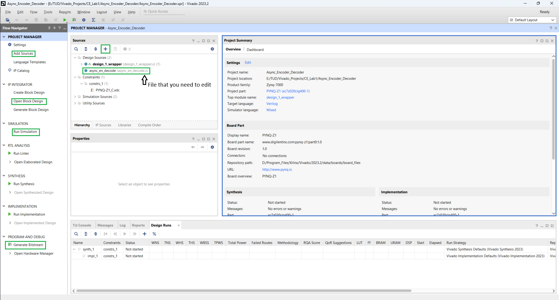
Above you can see the file async_en_decode.v, which needs to be edited to complete the assignment. Other functions that you will be using in the lab are also highlighted.
You can now Open the Block Diagram. A block diagram is a visual representation of all the interconnected IPs and Verilog blocks with each other and with external components. The block diagram for this project is shown below.
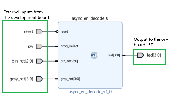
There are 3 main parts to the above block diagram.
- Inputs coming into the block diagram from the board. These include:
- Reset switch: Mapped to SW1
- SW switch: Mapped to SW0
- Binary Rotary Encoder: Mapped to PMODB[0:2]
- Gray Encoder Switch: Mapped to PMOD[4:7]
- In the middle is the RTL code you will write in the Verilog file.
- Finally, the output LEDs are mapped to the on-board LEDs
The above-mentioned component mapping is done in the constraints file. This file is located in Sources -> Constraints -> constrs_1 -> PYMQ-Z1_C.xdc. You can open and explore how the physical pins on the FPGA are mapped to various external components. These files are different for every development board, based on the on-board components.
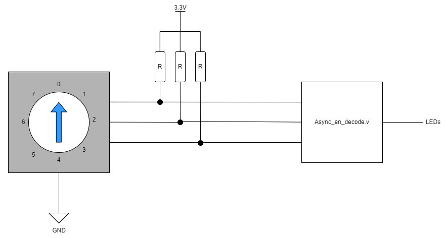
Step 1: Binary Display
Now that you are a bit more familiar with the Vivado tool. Open the async_en_decode.v file. In this exercise, you will be mapping the binary input from the binary rotary switch to the on-board LEDs.
Follow the following steps to complete the assignment:
- Make an asynchronous
always@(*)block in the module - Implement the reset switch logic:
- If the
resetsignal is on, your code should turn off all the LEDs - Only if
resetis off, the rest of the code should be executed
- If the
- Map the
bin_rotinput to theled[2:0]output. Refer to the circuit diagram below.- Note: The rotary switch is connected with pull-up logic
- Make a testbench for your project and simulate.
- You can find the steps to making your testbench in Simulation & Synthesis
- Once you have the testbench working as expected you can move on to Step 2
The data sheet for the binary rotary switch being used: Binary Rotary Switch (S-8010)
Step 2: Cardinal Direction Decoder
In this exercise, you will interface with the gray rotary switch and convert the inputs from the gray rotary switch into Cardinal directions.
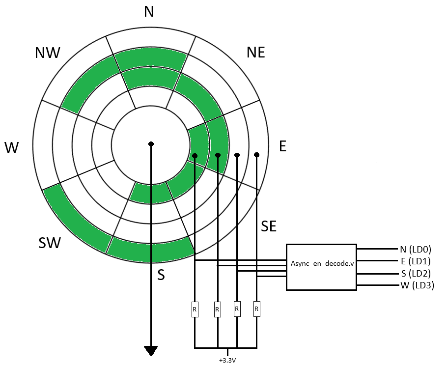
As you can see from the above image, you have to translate the rotary switch output into cardinal directions. For example, if the wheel is in the North position, only LD0 should be on and if the wheel is in the South-West direction, then both LD2 and LD3 should be on.
Follow the following steps to complete the assignment:
- Since you are going to use the same project for 2 programs, you need to use the
prog_selectswitch- When the switch is
UPthe binary display from Step 1 should be executed - When the switch is
DOWNthe Cardinal Direction Decoder should be executed
- When the switch is
- Implement cardinal direction decoder logic in
async_en_decode.v - Modify the testbench to test cardinal direction decoder logic
- Once successfully tested, generate bitstream, and program the FPGA to test binary display
- Call a TA to test your final design and test your cardinal direction decoder on hardware
The data-sheet for the gray rotary switch being used: Grey Rotary Switch
Part 2: Debouncing of electrical signals
In this lab, you will work with the on-board buttons and make a binary and gray-encoded counter.
Learning Goals of the Lab
- Interface with buttons on the board
- Use Debouncing and understand its need
- Implement synchronous logic
- Programming and testing the FPGA
Step 1: Binary Counter
In this step, you should implement a synchronous binary counter, and display the value using the on-board LEDs. When BTN0 is pressed, the counter should increment, and BTN1 is pressed the counter should decrement.
Note: Do not forget to implement the reset logic, similar to Part 1
- Open the
Debouncerproject in Vivado - Implement synchronous logic to increment and decrement the counter and display it on the LEDs
- DO NOT modify the block diagram yet
- Write a testbench for the module and simulate it using the simulation tool in Vivado
- Generate bitstream and upload it to the FPGA
Did the counter work as expected? Read more about what is debouncing and why do we need it: Debouncing
Step 2: Adding Debouncing
Here, we introduce debouncing logic in our project. This should remove all issues with your program getting multiple button presses.
- Open the Block-Diagram
- Disconnect the encoder
A&Binputs from the buttons - Connect the inputs to the
btn_outof the debouncer block - Simulate to verify that you have made the connections correctly
- Generate the bitstream and program the FPGA
Step 3: Converting to Gray Encoding
In this step, you will convert your binary value into a gray encoded value and display it on the LEDs
- Add an additional asynchronous block to convert the binary value into a gray encoded value
- Use an internal register to store your binary value
- You can use a look-up table for the conversion or use the gray encoding equations for 4-bit numbers
- Simulate to verify that you have made the encoding correctly
- Generate the bitstream and program the FPGA
Note: You can refer to Gray Encoding.
Once completed, please call the TAs who will approve your work and you can continue with the rest of the lab.
Part 3: Finite State Machine (FSM)
In this part, you will be implementing an FSM for a Road Safety Sign. The particular sign that you need to implement has the following modes:
- Arrow Point Left
- Arrow Point Right
- Blinking Lights Warning Mode
- Safe Mode

Learning Goals of the Lab
- Understanding and Implementing a Finite state machine
- Understanding different components and types of FSMs
To complete this exercise, use the Road_Sign provided in the template folder. Open it using Vivado. You will need to modify Road_Sign\Road_Sign.srcs\sources_1\new\road_sign.v to implement the encoder.
Step 1: Circular FSM
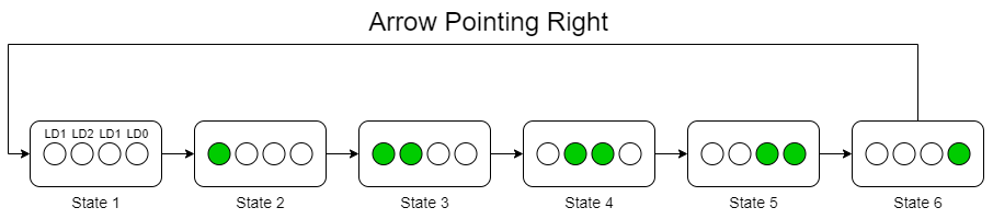
First, you will implement only the Arrow Pointing Left Mode. In this mode, the LEDs light up in a sequence moving towards the left. This is used to let the people know to divert to the left side of the road.
Since we have only 4 LEDs on the board, a pattern of running left LEDs is used to point left. For this, you will implement a 6-state circular FSM that has the following states:
![]()
For the FSM to switch between the states, we have a time constraint. Every state transition should take place after 500ms. To achieve this, you can use the provided clock which is of 125MHz, and divide it appropriately so that the state update happens when expected.
Step 2: High-Level FSM
Once you have Point Left working correctly, you need to implement a higher-level FSM to control which mode the Road Sign is in.
To complete this step follow the following steps:
- Make an independent 4-state FSM
- The 4 states are Point-Left; Point-Right; Warning; Idle
- The FSM state change is triggered by the 4 on-board buttons. When the corresponding button is pressed the FSM should enter that mode
- Point-Left: BTN0
- Point-Right: BTN1
- Warning: BTN2
- Idle: BTN3
- Before implementing the functionality of these states, verify that the high-level FSM is working as expected
- Use the RGB_LED1 to verify your functionality (Map 1 color to each state)
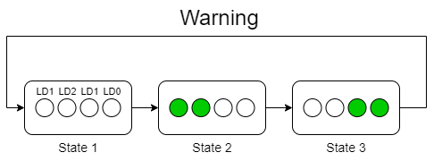
- Duplicate the circular FSM used before and use it for Arrow Point-Right and Warning. As shown in the below figures
- In the Idle state ensure that all the LEDs are turned
OFF.
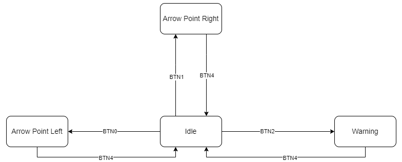
Step 3: Introducing Safe State of Execution
In the High-Level FSM implemented in the last step, any state can enter any other state. Which is a very unsafe way to transition between states. Since the road sign is deployed in a hazardous outdoor environment like a road-work site, it is important to have an additional safety measure. This can prevent accidental changes in the state of the sign, which can be hazardous on an active highway for example.
Thus, you need to add a constraint to the high-level FSM. You need to ensure, that if the FSM is in Point-Left, Point-Right, or Warning State it can only go to Idle state. And when in the Idle state it can enter any other state. A basic FSM diagram is presented below:
BONUS: Linear Feedback Shift Register Random Number Generator
What are LFSRs:
Linear Feedback Shift Register(LFSR) is a commonly used method to generate a set of pseudo-random numbers since it theoretically will be able to cover all the possible inputs for any n-bit circuits. A schematic of a typical LFSR is demonstrated in the figure below. A characteristic polynomial demonstrates the representation of the structure of the LFSR.
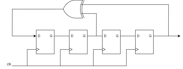
In this example, the characteristic polynomial is \(P(x)=x^4+x^2+1\), which indicates that the first bit will be the XOR result of the 4th and 2nd bit. Repetition distance stands for the number of cycles that the two same generated pseudo-random numbers appear twice. To get the cycle counter, you will implement an internal counter to record the cycle. Seed it as the initial value of the internal register after you press the "reset" button.
Lab Procedure
Implement a 6-bit LFSR with the polynomial of \(P(x)=x^6+x^5+x^3+1\), with three seeds, different seeds.
| Seeds Stored |
|---|
| 6'b00_0000 |
| 6'b01_1001 |
| 6'b10_1001 |
Follow the steps below to complete this lab:
- Open Vivado and make a new project (no template is provided for this part)
- Instructions on making a new Vivado project can be found in Vivado Project Setup.
- Implement a LFSR logic with the polynomial \(P(x)=x^6+x^5+x^3+1\) in the project
- Add logic to check when the LFSR loops back and starts repeating the sequence
- We recommend having a repetition signal as an output, it can go high when the LFSR value is the same as the seed value
- Write a testbench to test the LFSR Implementation
- Simulate the LFSR using the 3 seeds mentioned above
- Record the repetition distances for all three seeds
Once you have finished the simulation, please call a TA for implementation verification.
This guide is supposed to only be followed by groups that cannot install vivado on their computer.
Connecting to the Computer Engineering server
You will be using borrowed access to the Hardware Fundamentals (CESE4005) lab server. Beware that ssh connections can be slow depending on the internet connection, so be patient.
- Communicate that you do not have Vivado with one of the TA's to get your group's sign in information.
- On your machine or on the laboratory machine, download MobaXterm Portable edition.
- Open a local terminal and log in through ssh with X forwarding:
ssh -X cese4005-<grp-nbr>@ce-hwfund.ewi.tudelft.nl. Where<grp-nbr>is your group number, and fill in your password given to you by the TA's. - Move the vivado template project files from the
/coursedirectory to your home directory, so you are able to modify them. You can do this by runningcp -r course/. ~. An error will probably appear that some log files cannot be copied, you can ignore this. - Type
vivadoin the terminal to start Vivado. Open and change the project as you would on your local machine.
You are able to simulate any design you make, but once you are done with the Debouncer, generate the bitstream and upload it to the following OneDrive folder, inside your group folder , and come to the TA's to test it on the FPGA. The generated bitstream is located in the <lab-name>/<lab-name>.runs/impl_1 directory.
Lab1: Setup
Please ensure that you have Lab Setup completed before the lab
Vivado Installation
To run the labs it is recommended to install Vivado and Vitis (you will also need them in the Processor Design Project in Q4), but if you absolutely cannot install them, contact the TAs so they can arrange access to a remote server. The entire installation requires between 50 to 60 GB of disk space.
Installers are available for Linux and Windows: https://www.xilinx.com/support/download. The coming lab was tested in version 2023.2 (and likely works in 2024.1). After you click on download, you need to create an account or log in if you already have one. On Linux do not forget to allow running chmod a+x FPGAs_AdaptiveSoCs_Unified_2023.2_1013_2256_Lin64.bin and ./FPGAs_AdaptiveSoCs_Unified_2023.2_1013_2256_Lin64.bin
For Mac users we are trying to find the best solution. The site will be updated, once we have tested an installation approach.
Once you run the installer:
- Select Vitis
- Select the minimal installation components as shown in the image below. Windows: leave the last option (Cable drivers) checked.
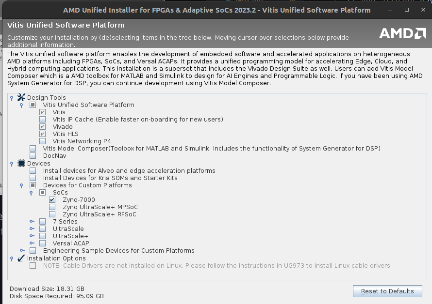
- Linux: install cable drivers by running:
cd ${vivado_install_dir}/data/xicom/cable_drivers/lin64/install_script/
install_drivers/
sudo ./install_drivers
Read more about Cable Drivers: https://docs.amd.com/r/en-US/ug973-vivado-release-notes-install-license/Install-Cable-Drivers.
After the installation is complete, ensure that you have Vivado 2023.2 and Vitis Classic 2023.2 installed.
If you face any issues with the installations please reach out to the TAs. You will not be able to start working on Lab 1 without the software completely installed. So you must install it before the lab so you don't lose time during the lab.
Installing a Serial Terminal
Only required for Lab 2, but recommended you install before the labs
A serial terminal is required to display the data sent back from the FPGA. There are many options for a serial terminal, any one of them is acceptable. A few recommended programs are listed below:
- Putty (Suggested for new instals)
- MobaXTerm
- Ardunio IDE
- Termite
Lab Hardware
In Lab 1 and Lab 2 you will be using the PYNQ-Z1/Z2 (reference manual) Development Boards by Digilent
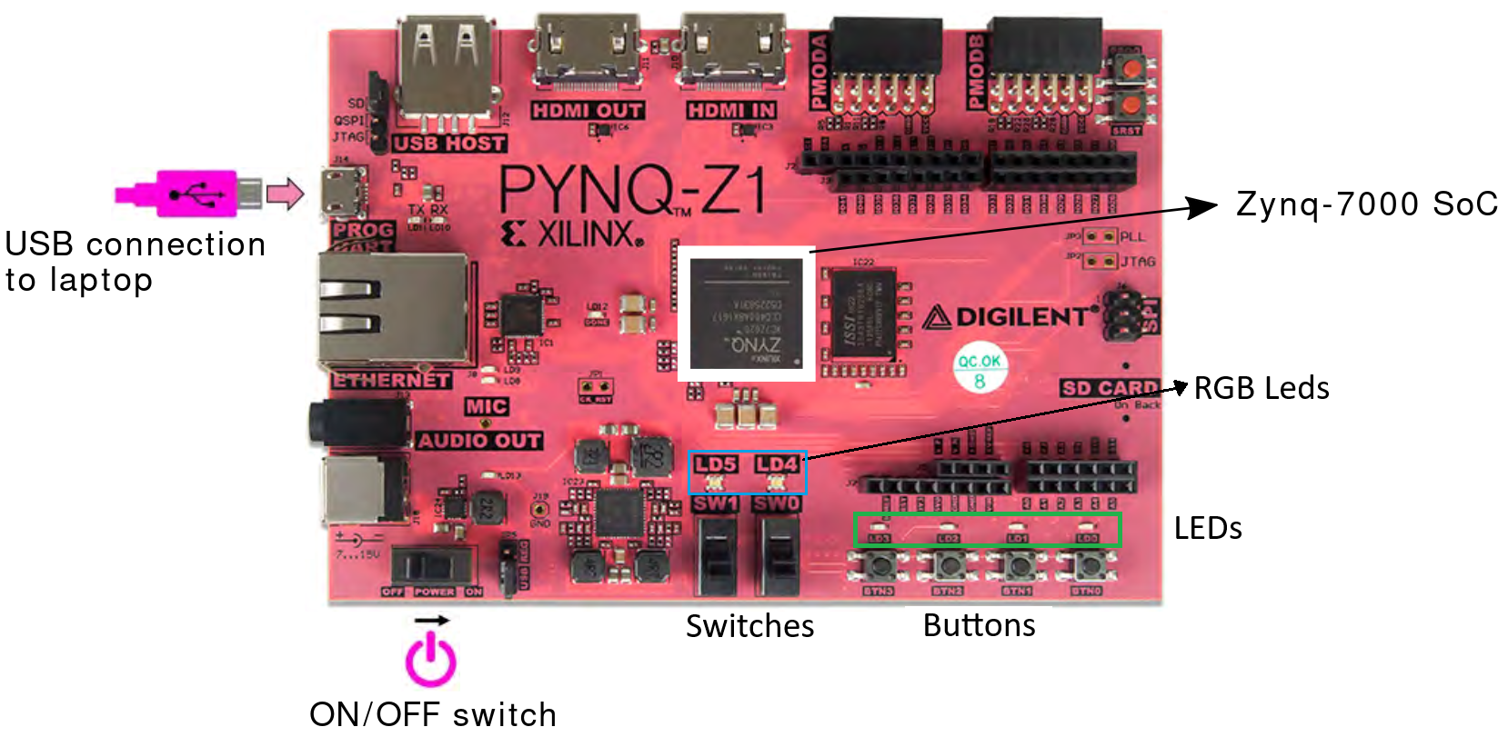
On this board, there's a Zynq-7000 SoC chip (reference manual), which is divided into two distinct subsystems:
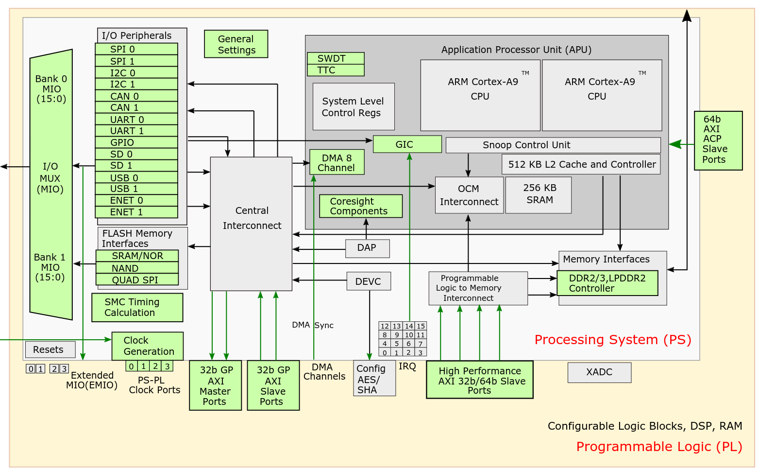
- The Programmable Logic (PL), which includes an array of programmable logic blocks and a set of dedicated resources (e.g., block RAM memories for dense memory requirements, DSPs for high speed arithmetic, analog-to-digital converters)
- The Processing System (PS), whose key components include:
- hard silicon ARM Cortex-A9 processors
- clock generators
- DDR and memory controllers
- I/O peripherals (e.g., GPIO, UART)
- PS-PL connectivity interfaces.
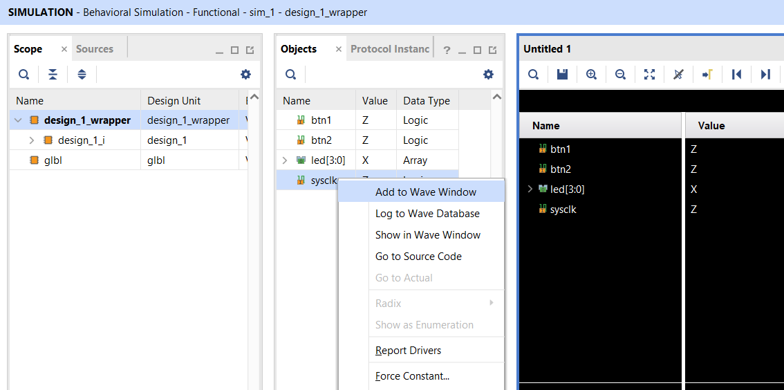
Simulation & Synthesis
Simulation
Simulation is an important step when working on any FPGA project. It lets you test your code with custom inputs and access all the variables within your code. Additionally, for bigger projects, simulation has a much faster turn-around time rather and synthesizing your design and running it on the FPGA.
To simulate your project:
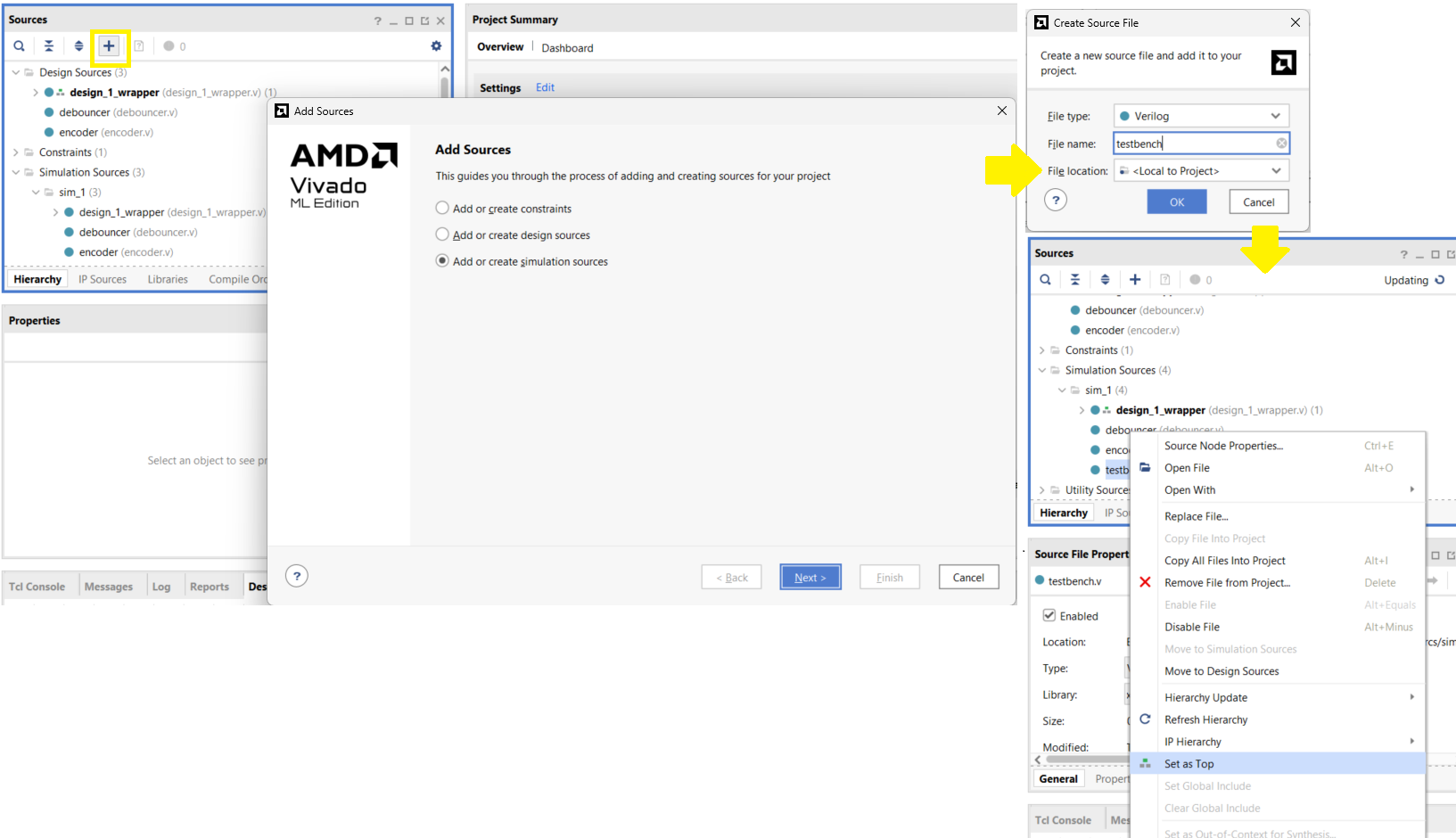
- Create a new testbench file
- With the project Open, select
Add Sourcesor pressAlt + A; selectAdd or create simulation sources - Select
Create File, name the filetestbench, thenFinish - Expand
Simulation Sourcesin theSourceswindow. - Right-click on your testbench file and select
Set as Top. Your testbench file name should be written in bold
- With the project Open, select
-
Write your test-bench
- Create an Instance of the module you want to test.
- Add code to modify the inputs to check various cases
- If the module under test has synchronous logic, simulate a clock signal in your testbench
// General testbench example `timescale 1ns / 1ps module testbench; reg clk; // Inputs as reg and outputs as wire reg reset; reg [3:0] input_signal; wire [3:0] output_signal; your_module uut ( // Instantiate the unit under test .clk(clk), .reset(reset), .input_signal(input_signal), .output_signal(output_signal) ); initial begin // Clock generation block clk = 0; forever #5 clk = ~clk; // Invert clock signal every 5 time units end initial begin // Stimulus block reset = 1; // Initialize inputs input_signal = 0; #10; // Wait to un-toggle reset reset = 0; #10 input_signal = 4'b0001; // Test inputs #10 input_signal = 4'b0010; #10 input_signal = 4'b0100; #10 input_signal = 4'b1000; #50; // Wait and finish $finish; end endmodule -
Simulating your design
- Launch the simulation by selecting,
Flow Navigator -> SIMULATION -> Run Simulation -> Run Behavioral Simulation. - When the simulation you defined in your testbench is complete, open the waveform viewer to view your signals.
- You can add more signals to the
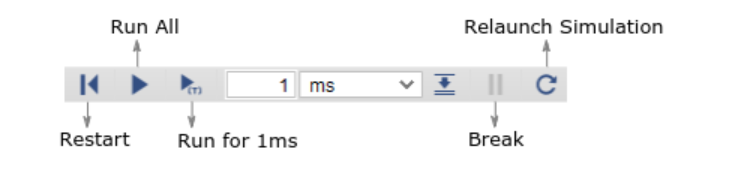
Wave Window. You can find more by expanding theSourceson the left side of the window. After you add a new signal you must reload the simulation to see the new signal changing. - Use the controls on the top taskbar to start/stop the simulation
- Do not forget to resize your simulation window, so you can see the signals for the entire duration of the simulation
- Launch the simulation by selecting,
Running Project on FPGA
Once the project is working as expected in the simulation, you need to generate the bitstream to upload to the FPGA.
Run Program on the FPGA:
-
Generate Bitstream
- Select
Flow Navigator -> PROGRAM AND DEBUG -> Generate Bitstream - This will generate the bitstream for your project. This step may take up to 5 minutes to complete. So prefer the simulation to verify the correctness of your code.
- Select
-
Connecting to the FPGA
- Connect the FPGA to the Laptop using the USB Cable and turn ON the FPGA switch if it is OFF
- In Vivado select
Flow Navigator -> PROGRAM AND DEBUG -> Open Hardware Manager - Select
Open targetat the top of the window, then selectAuto Connect
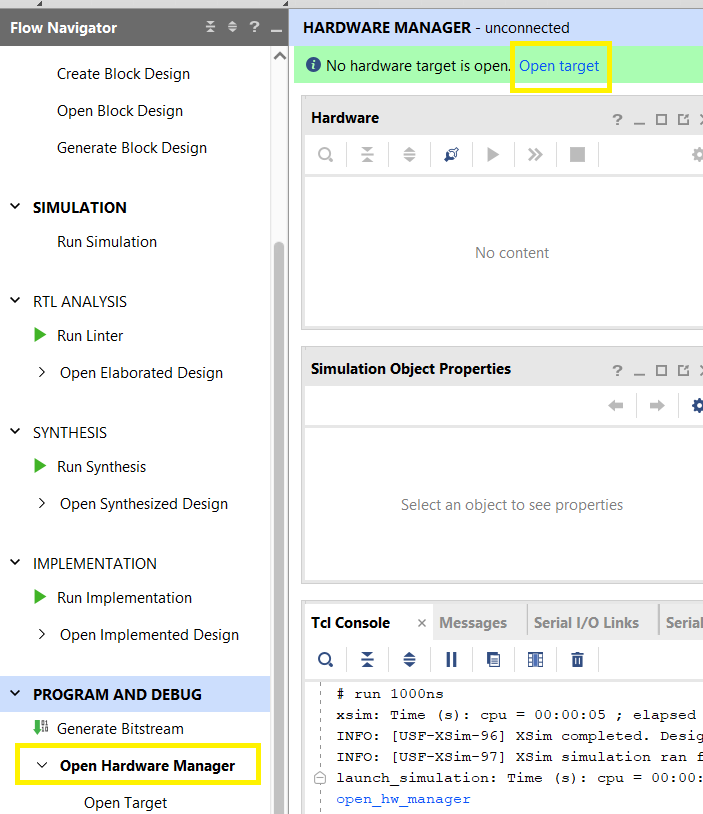
-
Program the FPGA
- Right-click on the FPGA, select
Program Device - Select the bitstream that was generated in the previous step. It can be found in
<project_name>\<project_name>.runs\impl_1. - Program the FPGA
- Right-click on the FPGA, select
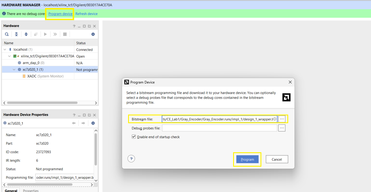
Your FPGA is now programmed and running the Verilog code that you wrote!
Vivado Project Setup
Creating a Project
To generate a new project in Vivado follow the steps:
- Download the Board files from here and paste them into
{installation_location}\Xilinx\Vivado\2023.2\data\boards\board_files\ - Start
Vivado, SelectCreate Project - Name your project and select
Next - Select
RTL Projectand ensure,Do not specify sources at this timeis selected - Select
Boardsand search forPYNQ-Z1; Select the board from the list and clickNext - Click
Finishand your project is completed
Setting up a Project
First you need to add the constraints file for the selected board. For the PYNQ-Z1 board follow the following steps:
- Add the constraints file for the board from the template repo,
PYNQ-Z1_Constraints.xdc. Press the+button in the Sources Tab or PressALT+A - Select
Add or create constraints, add the file downloaded in the previous step, and selectFinish - The constraint file has all the available GPIOs, LEDs, Buttons, and Switches on the board. You need to uncomment the ones you will need for the project.
- PYNQ-Z1 also provides a 125MHz clock, enable it and use it in your design.
Second, you will have to either add or create a new source file. This can done similarly to the constraint file but by selecting, Add or create sources. A source file is an Verilog file, in which you write your code. Ensure that the inputs and outputs of the Verilog module are set correctly.
Third, you will have to create a new block diagram. Block Diagram is used to stitch different IPs and components together in your project. To create a block diagram select Flow Navigator -> IP Integrator -> Create Block Diagram. You can now add your Verilog source to this block diagram by right-clicking on the file and selecting Add Module to Block Diagram. If you want to connect any pins from your block to external GPIOs, you can right-click on them and select Make External or press Cntr + T.
Ensure that the names of the resources in the constraint file and the block diagram are the same.
Fourth, and finally, once your block diagram is completed Right-click on it and select Create HDL Wrapper.... This will make an additional Verilog file which will act as the top layer of your project connecting all the IPs and sources in the block diagram together.
Now the project can be simulated or bitstream can be generated.
Lab 2: RISC-V
Welcome to Lab 2, a medium-sized Verilog project focused on FPGA development using Vivado. In this lab, you will be working with a custom RISC-V CPU core and implementing a Scaled Index (SI) load instruction to extend its functionality.
DOWNLOAD THE TEMPLATE : PicoRV32_template. Inside you will find a Baseline project, which you will use to implement the new instruction.
IMPORTANT VIVADO NOTE : When you make any changes in the Verilog file, you need to open the block diagram and
Refresh the Changed ModulesORUpdate IP. If not done your generated bitstream will be built using the OLD Verilog code. This is a Vivado tool requirement and we cannot do anything about this.
Table of Content
- Lab Evaluation Method
- Part 1: Understanding RISC_V and PicoRV32 core
- Part 2: Adding an instruction
- Part 3: Testing and Profiling the new instruction
- BONUS: Answer the following Questions
Learning Goals of the Lab
- Introduction to RISC-V Architecture
- Understanding how instructions are executed on a processor
- Implementing a custom instruction and understanding the impact of this
- Introduction to Vitis Classic and understanding how memory works in Vivado
Lab Evaluation Method
Each Part of this Lab has questions that you need to answer as a GROUP. Once you have finished a Part, you can answer the questions and call a TA to get it verified (if TAs are busy and you are confident in your answers, you can move on to the next Part, but get it verified before the end of the lab session).
We suggest you carry pen and paper (or note-taking tablet) with you to the lab to answer these questions.
Part 1: Understanding RISC-V and PicoRV32 core
You may do this part of the assignment before the lab session.
The link to download the template is provided at the beginning of this page!
In this section, you will understand how RISC-V instructions are structured and how the PicoRV32 executes an instruction. Answer the following questions and once completed, call a TA for sign-off.
- Decode the following instruction and write it in assembly format using RISC-V Instruction Card and RISC-V Register Map
32'b00000000000100111110111010010011
- Convert the assembly code into binary machine code, with clear demarcation for the various sections of the instruction using RISC-V Instruction Card and RISC-V Register Map:
add t0, a2, s3
-
Understanding the
load_wordinstruction implementation in the PicoRV32 Processor(a). What two local registers are used to uniquely identify the load word instruction? What fields of instruction are used for this? (You can refer to PicoRV32 Instruction Decoder)
(b). Draw a block diagram showing all the CPU state transitions involved in a load word instruction where the first and last cpu-state is
fetch. (You can refer to PicoRV32 CPU States)(c). What does the
cpu_state_ldmemdo? List all the instructions that use thiscpu_state_ldmemstate as part of their execution (Refer topicorv32.vline no1856)
Part 2: Adding an instruction
In this Part, you will be adding a Scaled Indexed Load instruction, formally known as Load Word Indexed (LWI) (not "immediate" if you are familiar with MIPS assembly). To add this custom instruction to the RISC-V core, you will have to modify the Verilog code of the processor. The processor should be able to decode the new instruction and execute the expected operation when the instruction is called.
Understanding the Template
The link to download the template is provided at the beginning of this page!
The template provided has additional components other than the PicoRV32 core. You should read through the Project Structure section to get a better understanding of how the project works and how the PicoRV32 core executes code.
Running the Baseline
For groups who do not have Vivado installed in their laptops, you can use the desktops in the Lab. To use the desktops, follow the steps explained in Using the Desktop
Before making changes in the code, you should try simulating the baseline project. Please follow these steps:
-
Read and understand the baseline code shown below:
1 _start: 2 # Load base address of 0x4000_0050 into t0 3 lui t0, 0x40000 # Load upper 20 bits of address into t0 4 addi t0, t0, 0x50 # Add lower 12 bits of address to t0 to get 0x4000_0050 5 6 # Load the value at address 0x4000_0050 into t1 7 lw t1, 0(t0) # Load the 32-bit value from address 0x4000_0050 into t1 8 9 # Load the value at address 0x4000_0054 into t2 10 lw t2, 4(t0) # Load the 32-bit value from address 0x4000_0054 into t2 11 12 # Perform addition 13 add t3, t1, t2 # Add t1 and t2, store result in t3 14 15 # Infinite loop with nop instructions 16 loop: 17 nop # No operation 18 j loop # Jump to the start of the loop -
Open
testbench.vand verify that it reads the baseline memory as below and save the file. This will ensure that the simulator loads the unmodified memory module.57. // Baseline ISA 58. $readmemh("memory_data.mem", mem.memory_array); -
Follow
Flow navigator → SIMULATION → Run Simulationand wait until you see the wave outputs. -
By looking at the OPCODE signal, you can verify that instructions are being decoded one after another. There is no need to manually decode the instructions.
-
Note down the values stored in t2 and t3. Right click on the signal to change radix. And compare with the Expected Simulation Output.
LWI Instruction
The Indexed Load instruction, described by the opcode 0101011, is used for advanced memory addressing techniques. It uses rs1 and rs2 to calculate the effective memory address. Two registers instead of one and an offset when compared to the lw instruction.
The lwi instruction, short for "Load Word Indexed" has a specific encoding in the RISC-V instruction set. The instruction is encoded as follows:
| 31 ... 25 | 24 ... 20 | 19 ... 15 | 14 ... 12 | 11 ... 7 | 6 ... 0 |
|---|---|---|---|---|---|
| funct7 | rs2 | rs1 | funct3 | rd | opcode |
| 0000000 | rs2 | rs1 | 010 | rd | 0101011 |
- func7 (7-bits): A constant field containing
'0000000'. - rs2 (5-bits): Specifies the index register.
- rs1 (5-bits): Specifies the base register.
- func3 (3-bits): A constant field containing
'010'. - rd (5-bits): Specifies the destination register.
- opcode (7-bits): The opcode for this custom instruction containing
'0101011'.
Additional Information about the RISC-V Instruction structure is provided in RISC-V Card
LWI Assembly format:
'lwi <rd>,<rs2>(<rs1>)'
Here the <rd>, <rs1>, and <rs2> placeholders denote the fields which specify the destination, base, and index registers, respectively.
LWI Assembly example:
0: 0x16A232B lwi t1, s6(s4)
Operation
The operation for this instruction can be represented as the following C code:
void lwi(uint32_t rs1, uint32_t rs2, uint32_t &rd) {
    rd = *(int32_t*)(rs1 + rs2);
}
- Note: The index is not word scaled: it is byte-scaled. This means that the value in rs2 is treated as a byte offset rather than a word offset. To access the n-th 32-bit element in an int array, for example, you would need to set
rs2ton * 4, not simply n.
Assignment Steps:
Make modifications in the picorv32.v file to add the custom instruction. These changes are divided into 3 steps (Refer to your answers for Part 1: Q3 ):
- Modify the instruction decoder of the processor to decode and recognize the instruction.
- Modify the CPU state transitions to enter the correct mode when the new instruction is detected.
- Modify the
cpu_state_ldmemor create a custom-defined state to execute the operation for the custom instruction.
Hint: If you are having issued with the above steps, start by understanding how
lw(Load Word) instruction is decoded and implemented.
Running the Modified Code
After implementing the LWi instruction in the Verilog code, it is time to simulate and verify its functionality. Follow the steps below:
-
Read and understand the code which uses LWi in action:
1 _start: 2 # Load base address of 0x4000_0050 into t0 3 lui t0, 0x40000 # Load upper 20 bits of address into t0 4 5 # Load the value at address 0x4000_0050 into t1 6 addi t1, x0, 0x50 7 lwi t2, t1(t0) # Load the 32-bit value from address 0x4000_0050 into t1 8 9 # Load the value at address 0x4000_0054 into t2 10 addi t1, t1, 4 11 lwi t3, t1(t0) # Load the 32-bit value from address 0x4000_0054 into t2 12 13 # Perform addition 14 add t3, t3, t2 # Add t1 and t2, store result in t3 15 16 # Infinite loop with nop instructions 17 loop: 18 nop # No operation 19 j loop # Jump to the start of the loop -
Open testbench.v and verify that it reads the modified memory as below and save the file. This will ensure that the simulator loads the modified memory module. Do not forget to comment the baseline memory module.
57 // Baseline ISA 58 // $readmemh("memory_data.mem", mem.memory_array); 59 60 // Modified ISA 61 $readmemh("mod_memory.mem", mem.memory_array); -
Follow
Flow navigator → SIMULATION → Run Simulationand wait until you see the wave outputs. -
By looking at the OPCODE signal, verify that you can see the LWI opcode bits.
-
Note down the value stored in t3. Compare with the Expected Simulation Output in the Simulation section.
Only then, Generate the Bitstream and program the FPGA. Refer to Synthesizing & Programming and the following instructions to program the FPGA.
Groups using the Lab desktops follow the instructions in Flashing FPGA from the Desktop, to program the FPGA from the Desktops.
Groups facing issues with Vitis Classic. Follow the step mentioned in Running remotely to run your program.
Note: Do not forget to note down number of cycles before you pass on the FPGA to the next group.
Part 3: Testing and Profiling the new instruction
Once you have the instruction implemented, it is important to understand how the new instruction can be used in a real-world application.
Answer the following questions based on your observations from the simulation and serial log:
-
How many cycles are required for the
lw,add, andlwiinstructions in simulation? -
Refer to the img_blur code for Baseline implementation and Modified implementation and calculate the theoretical difference in cycle count between the two programs.
- Hint: Given that our image is 32x32 pixels the blur loop will run 1,024 times
-
What is the actual difference in cycle count you noted down at the end of Part 2 when the Baseline and Modified programs are run on the FPGA?
-
When you compare your theoretical difference in cycle count with the actual difference, you can see that they do not match. This is because simulation is only an abstraction of the actual system. The memory is connected directly to the processor in the simulation, but on the FPGA it goes through many intermediatory components. You can see that in the Block Diagram.
Given that, reading an instruction from the instruction memory takes four more cycles for each instruction, and each time you load a value from the memory it takes one more cycle.
Recalculate your theoretical cycle counts now. Do they match?
BONUS: Answer the following questions
-
Why is image blurring a good use of the
lwiinstruction, suggest 2 more algorithms that can benefit from this instruction. -
Suggest a new custom instruction that can also optimize the image blurring program. Justify your answer.
-
How will the ratio of cycle count in baseline vs modified change, if the number of pixels is increased? Justify your answer.
-
Area Utilization (To answer this question Refer to Area Utilization Report):
(a). Does the added instruction significantly increase slice utilization? (for more information: FPGA Slices)(b). How might this affect scalability or the addition of further instructions in the future?
Project Structure
In this section, we explain how the RISC-V PicoRV32 core is implemented in the PYNQ Z-1 FPGA Board.
Block Diagram
The block diagram is a high-level design for all the components implemented on the FPGA.

High-Level Components
- system_reset: Reset the complete FPGA
- picorv32_reset: Reset only the RISC-V core
- ZYNQ Processing Systems: A hardwired ARM core within the FPGA. It is used to program and validate the RISC-V Core.
- picorv32_processor: RISC-V Core
- memory_block: Contains the Instruction (ROM) and Data (RAM) for the RISC-V core
- processor_interconnects: Used to connect the 2 cores with the memory and external GPIOs
How a Program runs on the RISC-V Core
The hardwired ARM core is used to interact with the RISC-V core. Following are the steps to run and validate a program on the RISC-V core.
- The FPGA is initialized and all the memory blocks are reset
- The ARM core loads the instruction and data memory with RISC-V machine code
- The RISC-V core is reset and executes the program according to the instructions in the instruction memory
- The ARM core waits till the RISC-V core is finished execution.
- The ARM core validates the output of the RISC-V core, which is stored at a pre-defined address in the data memory.
- A green LED indicates successful execution, a red LED indicates a failed execution.
Note: Red_LD5 is connected to PicoRV32 trap signal. A trap is triggered when an incorrect instruction is read or the processor is in a deadlock situation.
Simulation
In this section, we explain the provided simulation and testbench setup, and how to use it. Since this is a complicated project, we provide you with a working testbench. It is assumed that you are familiar with Vivado Simulations, if not please refer to: Lab 1 Simulation & Synthesis.
The provided testbench.v consists of two main components
- picorv32 module: The core as a Unit Under Test
- memory module: A custom memory module for the core. RISC-V machine code (instructions) can be loaded into this memory.
Simulation programs
To simulate your core, you need a set of instructions for the core to execute (obviously). In the template, this is achieved by loading the memory module with RISC-V Machine code. There are two programs provided in the template, memory_data.mem which is compiled using Baseline ISA, and mod_memory.mem which is compiled with the new instruction (Modified ISA).
Choosing a program
Before simulating you need to select which program you want to simulate. This can be done by uncommenting one of the $readmemh instructions, as shown below.
56
57    // Baseline ISA
58    $readmemh("memory_data.mem", mem.memory_array);
59
60    // Modified ISA
61    //$readmemh("mod_memory.mem", mem.memory_array);
62
To ensure that your simulation is executing correctly, validate your results against Expected Simulation Output bellow.
Expected Simulation Output
Both the simulation codes perform the same operations. Verify that the final output Matches the following
| Register | Value |
|---|---|
| t3 | 44 |
When the register values match with the table above, that means the simulation has run successfully.
Synthesizing, loading and running the design
You don't need to do this step if you are only simulating the baseline
Only do this once you have successfully simulated the LWI instruction
Similar to Lab 1, you will Generate Bitstream using Vivado. But you will use Vitis Classic to program the bitstream not the Hardware Manager. In this project, you want to flash the bitstream and the code for the ZYNQ ARM Core, not only the bitstream we use the Vitis Classic.
Generating Bitstream and Exporting Hardware
Once your simulation is working with the new instruction. You can navigate to Flow Manager -> Generate Bitstream to generate the bitstream.
When the bitstream generation is completed, you need to export the hardware. To do this, select File → Export → Export Hardware..., click Next, select Include Bitstream option, and finish. This will export your *.xsa file, which is required for the Vitis project.
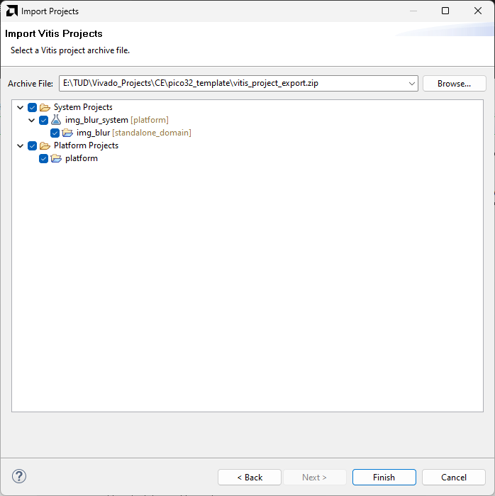
Setting up a Vitis Classic Project
Only need to do this step the first time launching Vitis Classic
Follow the steps to setup the Vitis Classic project required for this lab:
- Open Vitis Classic, select the
workspacefolder in project directory as the working directory - Select
File → Import... → Vitis project exported zip file - Browse and locate,
vitis_project_export.zipin the project files - Select Both system projects and platform projects and import
Flashing and Executing the Program
Once you have successfully generated and exported a bitstream and exported it using the Vivado tool, you can upload the new bitstream.
Follow the steps to program your FPGA:
- The hardware needs to be updated: Right-click on the
platformand selectUpdate Hardware Specification. Select the exported*.xsafile. - Once the platform is updated, Right Click on the
img_blurproject andBuild Project, and wait till the build is finished - Right Click
img_blur_systemand click onProgram Deviceand selectProgram - Launch a Serial Monitor and open the COM port with Baud rate 115,200.
- Right Click
img_blur_systemand click onRun As → 1 Launch Hardware
You should see the output from the FPGA on the serial monitor. Your output should be similar to the one shown below:
Successfully init
Starting Baseline ISA Test
Programming done
Program Completed with XXXXXX cycles
Image has been blurred correctly

Reseting the BRAMs

Starting Modified ISA Test
Programming done
Program Completed with XXXXXX cycles
Image has been blurred correctly
Note down the number of cycles taken by the Baseline ISA Test and the Modified ISA Test. You will need this to answer the questions.
Image Blur Program
For verification and profiling you will be using a custom Image blur program written in RISC-V assembly. To answer questions in the BONUS, you need to understand the assembly code. Both the original code and the modified (with custom instruction) are provided below.
The program performs image blurring of a 32x32 pixel black & white image. The image is padded with zero.
Expected Output
Since reading back the image from the FPGA is convoluted, we did it for you, and below are the expected results.
| Original 32x32 pixel image | Blurred Image |
|---|---|
 |  |
We are aware that this image blurring algorithm is naïve and not implemented optimally. The main goal of this program is to highlight the impact of
LWIinstruction.
Baseline Image Blur code
.global __start

.text

__start:
    # Actual Code starts here
bootloader:
    lui t0, 0x42000
    lw s2, (t0)	        # Load the image width
    lw s3, 4(t0)	    # Load the image height
    lw s4, 8(t0)	    # Pixel start address & loop counter
    li t2, 4
    addi s5, s2, 2		# Add padding on both sides
    mul s5, s5, t2		# Convert bytes to word
    neg s6, s5		    # -img_width
    addi s7, s6, 4		# -img_width + 1
    addi s8, s6, -4		# -img_width - 1
    addi s9, s5, 4		# img_width + 1
    addi s10, s5, -4	# img_width - 1
    li s11, 9		    # Number of pixels for blurring

    addi s0, s2, 0		# Set the row check
    addi s1, s3, 0		# Set the column check

    li a0, 0x42002000	# Store address for the blur image

blur:
    lw t0, (s4)	# Load pixel value (i)
    lw t1, 4(s4)	# Load pixel value (Right)
    add t0, t0, t1
    lw t1, -4(s4)	# Load pixel value (Left)
    add t0, t0, t1

    add t2, s4, s6	# Load pixel value (Up)
    lw t1, (t2)
    add t0, t0, t1
    add t2, s4, s7	# Load pixel value (Up-Right)
    lw t1, (t2)
    add t0, t0, t1
    add t2, s4, s8	# Load pixel value (Up-Left)
    lw t1, (t2)
    add t0, t0, t1

    add t2, s4, s5	# Load pixel value (Down)
    lw t1, (t2)
    add t0, t0, t1
    add t2, s4, s9	# Load pixel value (Down-Right)
    lw t1, (t2)
    add t0, t0, t1
    add t2, s4, s10	# Load pixel value (Down-Left)
    lw t1, (t2)
    add t0, t0, t1

    div t0, t0, s11	# Average the output (Divided by 9)

    # Store the output
    sw t0, (a0)
    addi a0, a0, 4

    # Check if the row is complete
    addi s4, s4, 4
    addi s0, s0, -1
    bnez s0, blur
    addi s4, s4, 8
    addi s0, s2, 0
    addi s1, s1, -1
    bnez s1, blur

    # Write the cycle count
    rdcycle t5              # Read lower 32 bits of cycle count into t5
    rdcycleh t6             # Read higher 32 bits of cycle count into t6
    lui t3, 0x42003         # Load upper immediate 0x42003 into t3
    addi t3, t3, 0x500      # t3 = 0x42003500 (target memory address)
    sw t5, 0(t3)            # Store the lower cycle count at 0x42003500
    addi t3, t3, 4          # t3 = 0x42003504 (next memory address for higher count)
    sw t6, 0(t3)            # Store the higher cycle count at 0x42003504

    # End of program (infinite loop with nop)
nop_loop:
    nop                     # No operation
    j nop_loop              # Infinite loop
Modified Image Blur code
.global __start

.text

__start:
    # Actual Code starts here
bootloader:
    lui t0, 0x42000
    lw s2, (t0)	        # Load the image width
    lw s3, 4(t0)	    # Load the image height
    lw s4, 8(t0)	    # Pixel start address & loop counter
    li t2, 4
    addi s5, s2, 2		# Add padding on both sides
    mul s5, s5, t2		# Convert bytes to word
    neg s6, s5		    # -img_width
    addi s7, s6, 4		# -img_width + 1
    addi s8, s6, -4		# -img_width - 1
    addi s9, s5, 4		# img_width + 1
    addi s10, s5, -4	# img_width - 1
    li s11, 9		    # Number of pixels for blurring

    addi s0, s2, 0		# Set the row check
    addi s1, s3, 0		# Set the column check

    li a0, 0x42002000	# Store address for the blur image

blur:
    lw t0, (s4)	    # Load pixel value (i)
    lw t1, 4(s4)	# Load pixel value (Right)
    add t0, t0, t1
    lw t1, -4(s4)	# Load pixel value (Left)
    add t0, t0, t1

    # Load pixel value (Up)
    lwi t1, s6(s4)
    add t0, t0, t1
    # Load pixel value (Up-Right)
    lwi t1, s7(s4)
    add t0, t0, t1
    # Load pixel value (Up-Left)
    lwi t1, s8(s4)
    add t0, t0, t1

    # Load pixel value (Down)
    lwi t1, s5(s4)
    add t0, t0, t1
    # Load pixel value (Down-Right)
    lwi t1, s9(s4)
    add t0, t0, t1
    # Load pixel value (Down-Left)
    lwi t1, s10(s4)
    add t0, t0, t1

    # Average the output (Divide by 9)
    div t0, t0, s11

    # Store the output
    sw t0, (a0)
    addi a0, a0, 4

    # Check if the row is complete
    addi s4, s4, 4
    addi s0, s0, -1
    bnez s0, blur
    addi s4, s4, 8
    addi s0, s2, 0
    addi s1, s1, -1
    bnez s1, blur

    # Write the cycle count
    rdcycle t5              # Read lower 32 bits of cycle count into t5
    rdcycleh t6             # Read higher 32 bits of cycle count into t6
    lui t3, 0x42003         # Load upper immediate 0x42003 into t3
    addi t3, t3, 0x500      # t3 = 0x42003500 (target memory address)
    sw t5, 0(t3)            # Store the lower cycle count at 0x42003500
    addi t3, t3, 4          # t3 = 0x42003504 (next memory address for higher count)
    sw t6, 0(t3)            # Store the higher cycle count at 0x42003504

    # End of program (infinite loop with nop)
nop_loop:
    nop                     # No operation
    j nop_loop              # Infinite loop
Code Hints
Below is the picorv32.v file with additional comments to help you understand where you need to make the required changes.
All the places where a modification is required is marked by: // Solution Lab 2:
Lab 3: Parallel processing
Welcome to lab 3, a lab that will introduce you to parallel processing using CUDA. You will learn how to write parallel programs that can run on a GPU, and how to optimize them for performance.
This is a preliminary version of the lab, and it is subject to changes until the lab date.
Table of contents
- Preparation
- Part 1: Matrix multiplication
- Part 2: Tiled matrix multiplication
- Part 3: Histogram shared memory
- BONUS
Preparation
Before this lab, you should have a basic understanding of C++, since it is the basis of CUDA programming. You should also have a basic understanding of parallel programming concepts, such as threads, blocks, and grids. To briefly review these concepts or see more information about CUDA programming, you can check This subset of CUDA Programming Guide, and This Even Easier Introduction to CUDA
Setup
If you have Linux and an NVIDIA GPU, we recommend you run the CUDA application locally on your computer. This will allow you to test your code faster and debug it more efficiently. Follow the CUDA local setup to install the CUDA Toolkit on your Linux machine.
If you do not have a CUDA capable GPU or Linux, you can use the DelftBlue cluster to run your code. Follow the CUDA DelftBlue cluster setup to access the cluster and run your code there.
For simplicity, this lab instructions are given for the DelftBlue cluster, but you can simplify them if you are running on your local machine
Submitting jobs on DelftBlue
After you have followed the CUDA DelftBlue cluster setup, you probably know that you can upload jobs by running the following command in the terminal: sbatch job.sh. Each part has their own job.sh file, so you can submit them separately. Once the job is complete you will get an output file with the results with the format ce-lab3-part<nr>-<job-id>.out. You can use cat ce-lab3-part<nr>-<job-id>.out to see the results. You can check the status of your job by running squeue -u $USER.
Warning: Do not upload the
job_backup.shfile, until explicitly told to do so by the TAs.
Part 1: Matrix multiplication
Objective
The purpose of this part is to implement a basic parallel matrix matrix multiplication algorithm in CUDA. The goal is to understand the basic concepts of CUDA programming, such as memory allocation, memory copying, kernel parameters and synchronization.
Procedure
- Inside your template folder, navigate to
square-matrix-multiplication. Here in main.cu, you will implement a CUDA kernel for matrix multiplication. Follow the following steps:- Allocate memory for the matrices on the device (GPU).
- Copy the matrices to the device.
- Define kernel parameters and call the kernel function.
- Implement the kernel function.
- Copy the result from device to host.
- Free device memory.
Hints: Understand the
CPU matrix multiplicationinmain.cuto implement something similar in your kernel. Refer to the lecture slides: CESE4130_9.
-
Once you have completed the code modifications, you can compile your code. To compile your code, first load the compiler using
module load cuda/12.5. Then you can usemaketo compile your code. -
Only when the code is compiled without any errors, upload a job to the DelftBlue cluster to run your code
sbatch job.sh. Wait for the results and analyze them as explained in Submitting jobs on DelftBlue.- Inside
job.shyou can change the line./matmultfor matrices with different sizes.1.
- Inside
Warning: Only use
verifyfor small matrix sizes, as it is not optimized for large matrices.
Once your program is correct answer the following questions:
Warning: You must synchronize after your kernel call, otherwise the time of your kernel will be inaccurate.
-
Examine the code output with a 16x16 matrix and compare CPU time vs. GPU kernel time. Which one is faster and why?
-
With the default BLOCK_SIZE of 32, find the number of: blocks, total threads, and inactive threads for the following cases (you don't need to run the code):
(a). 1024 x 1024 matrix size
(b). 2300 x 2300 matrix size
-
If we change the BLOCK_SIZE to 64 would the code still work? Why? You can briefly refer to the output of the
device-query -
For
./matmult 2048with BLOCK_SIZE values of 8 and 32. Find the number of blocks and compare the kernel times. Which is faster and why?
Once you are done answering the questions from this part, call a TA to verify your answers and proceed to the next part.
Part 2: Tiled matrix multiplication
Objective
The purpose of this part is to get familiar with shared memory use to optimize kernel algorithms. The goal is to implement a tiled version of the previous matrix multiplication routine in CUDA. You can learn more about shared memory here.
In this lab you will need to allocate shared memory for the tiles and copy the tiles from global memory to shared memory. You can copy unchanged parts from Part 1.
Procedure
- In the same template folder, navigate to
square-tiled-matrix-multiplicationand modify the kernel inmain.cuto implement the tiled matrix multiplication.
Hint: The lecture slides CESE4130_10 can be very helpful for this part.
-
Once you have completed the code modifications, you can compile your code. To compile your code, first load the compiler using
module load cuda/12.5. Then you can usemaketo compile your code. -
Upload a job to the DelftBlue cluster to run your code
sbatch job.sh, wait for the results and analyze them as explained in Submitting jobs on DelftBlue.- Inside
job.shyou can change the line./matmult-tiledwith different sizes.2.
- Inside
Once your program is correct answer the following questions:
Warning: You must synchronize after your kernel call, otherwise the time of your kernel will be inaccurate.
-
Find the speedup of tiled version vs. basic version (Part 1) for matrices with size 32, 128, 512. What is the maximum speed-up?
-
Is it true that tiled version is always faster than basic version? Why?
-
How does one handle boundary conditions in the tiled matrix multiplication when the matrix size is not a multiple of the tile size?
-
What role does synchronization play in the tiled matrix multiplication?
If you are having trouble with this part, you can check:
Part 3: Shared memory histogram
Objective
Now that you practiced with shared memory. You need to implement a histogram calculation in CUDA using shared memomry. This needs to be implemented using atomic operations.
Procedure
-
Inside your cloned directory, navigate to
character-histogram-shared-memoryand modify the kernel inmain.cuto implement the histogram calculation using shared memory. -
Once you have completed the code modifications, you can compile your code. To compile your code, first load the compiler using
module load cuda/12.5. Then you can usemaketo compile your code. -
Upload a job to the DelftBlue cluster to run your code
sbatch job.sh, wait for the results and analyze them as explained in Submitting jobs on DelftBlue.
Once your program is correct answer the following questions:
Warning: You must synchronize after your kernel call, otherwise the time of your kernel will be inaccurate.
-
Why does the histogram calculation require atomic operations? What happens if they are not there?
-
How would the choice of block size affect the performance of the histogram calculation?
-
Explain the use(s) of your
__syncthreads();
Hint: look at the commented out
verifyfunction insupport.cuto check how histogram calculation is done in the CPU.
Note: If you decide to stop your lab here, and you used VsCode proceed to closing down your connection to VSCode.
If you are having trouble with this part, you can check:
BONUS
Objective
The purpose of this part is to extend your tiled matrix multiplication to support non-square matrices. You will need to modify the code and the kernel in main.cu to implement the tiled matrix multiplication for non-square matrices.
Procedure
-
Inside your template folder, navigate to
bonus/rectangular-tiled-matrix-multiplication/, where you will, again, only need to modifymain.cufor setting up memory allocations and kernel code. -
Once you have completed the code modifications, you can compile your code. To compile your code, first load the compiler using
module load cuda/12.5. Then you can usemaketo compile your code. -
Upload a job to the DelftBlue cluster to run your code
sbatch job.sh, wait for the results and analyze them as explained in Submitting jobs on DelftBlue.- Inside
job.shyou can change the line./matmultwith different sizes.3.
- Inside
Once your program is correct answer the following question:
Warning: You must synchronize after your kernel call, otherwise the time of your kernel will be inaccurate.
- With the default BLOCK_SIZE of 32, find the number of: blocks, total threads, and inactive threads for
./matmult 1300 2 1300.
Note: If you used VsCode proceed to closing down your connection to VSCode.
-
./matmultUses the default matrix sizes 1000 x 1000,./matmult <m>Uses square m x m matrices. ↩ -
./matmult-tiledUses the default matrix sizes 1000 x 1000,./matmult-tiled <m>Uses square m x m matrices. ↩ -
./matmult-tiledUses the default matrix sizes 1000 x 1000,./matmult-tiled <m>Uses square m x m matrices,./matmult-tiled <m> <k> <n>Uses (m x k) and (k x n) input matrices. ↩
Lab 3: DelftBlue cluster setup
In this manual you will learn how to access your account in the DelftBlue high performance computing cluster created for this course. You should test if you can login into the server before the lab, to avoid any issues during the lab session.
Warning: In the DelftBlue cluster jobs are managed through a queuing system. So it is unpredictable to know when your job will execute.
Software
You can use any terminal application to connect to DelftBlue. Please note that if you are not using campus network, you have to use eduVPN first. Once you have connected to the campus network via either eduVPN or on-campus network, you can open your Linux/ Windows/ MacOS Terminal
How to connect
Depending on the software you have chosen, specify your NETID in the ssh command below, and run it in your terminal.
ssh <NETID>@login.delftblue.tudelft.nl
The login node then asks your TUDelft password, and after that, you should see the cluster prompt. Contact a TA if you have any issues. This step is essential to ensure your personal \home folder is created.
If you wish to use VSCode to connect and access your files through SSH. Follow the instructions in DelftBlue integrated development using an IDE
Download the template on DelftBlue
Run the following command to download the template and unzip it inside your \home directory.
curl https://cese.ewi.tudelft.nl/computer-engineering/docs/CESE4130_Lab3.zip --output CESE4130_Lab3.zip
unzip CESE4130_Lab3.zip -d CESE4130_Lab3
You are now ready to use the template.
Running the test on DelftBlue
Please use the following set of commands to run a simple device query test on the GPU node.
cd CESE4130_Lab3/device-query/
sbatch job.sh
After that run squeue -u $USER to check the job queue status. If the job is executed right after the sbatch command, due to its very short running time, you will see an empty queue. However, an empty queue doesn't always mean the job has been run successfully. If there is a problem with the script or command, the job manager will terminate the job right after the submission and again you will see an empty queue.
In the picture below, you see that: 1. The submitted job is in 'R' state which means the job is running on the target node; 2. The queue becomes empty. Please note that, if the target node is not ready yet, the job remains in the queue. This is specified with "PD" in the "ST" columns which means the submitted job is in pending state.

Once the queue becomes empty, an output file is generated in the folder and you can see the content with cat ce-lab3-part0-*.out. In a successful run, you should see device information, e.g. NVIDIA A100 or NVIDIA Volta specifications. If you see an error message in the output file, contact a TA.
You can now continue with the Submitting jobs on DelftBlue section.
Lab 3: Local CUDA setup
Only follow this instruction if you have a Linux system and a NVIDIA GPU. Please complete this before the lab!
This page will guide you through the setup of the CUDA toolkit and the compilation of a simple CUDA program.
CUDA Toolkit download
The CUDA toolkit 12.5 requires about 5GB of your system storage you can install it from the NVIDIA website CUDA Downloads. Choose the instruction that fits your system, and follow the instructions. An example for Fedora 39 is shown below.

Downloading the template locally
-
Open a terminal where you want your template to be and run
curl https://cese.ewi.tudelft.nl/computer-engineering/docs/CESE4130_Lab3.zip --output CESE4130_Lab3.zipto download the template. -
Unzip the template running
unzip CESE4130_Lab3.zip -d CESE4130_Lab3
Running device-query locally
-
cd /device-queryand runmaketo compile the program. -
Run the program with
./device-queryto check if everything is working properly.
DelftBlue integrated development using an IDE
To facilitate your lab, these instructions walk you through connecting remotely to an IDE, in this case, Visual Studio Code using SSH, so you can easily edit your code. The drawback is that you will have to manually kill your VsCode process after you finish the lab.
Note: You can easily use the terminal to run your commands, and Nano to edit (copy and paste) your code on the cluster. But if you prefer to use an IDE, follow the steps below.
-
Once you open VsCode, click on
Connect to...(or the blue><icon on the bottom left of the VsCode window) and selectConnect to host...from the dropdown menu.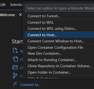
-
Select
Add new host...and login by typingssh <your-net-id>@login.delftblue.tudelft.nland your password. -
Select
Linuxand click onConnect. -
You can now access your home folder on your explorer (by putting your password once again) and opening a terminal to run your commands.
Warning: When you decide to close VsCode. Follow the instructions in Closing your VSCode connection.
Closing your VSCode connection
Note: This is meant for people that used the SSH connection through VSCode. If you used the terminal directly, you can skip this part.
The procedure is the following:
- Before closing VsCode, look in your VsCode integrated terminal to determine which login node you are connected to. It should be something like
login01,login02. - Open a new terminal on your computer and login to that specific login node using
ssh <your-net-id>@login0X.delftblue.tudelft.nlwhereXis the number of the login node. - Close the VSCode window.
- Run
top -u $USERin the ssh terminal to see the processes you are running. - Find the
code-<something>process and note its PID. If it is not present, you can close the terminal. And you are done! - If it is present. Kill it by pressing
kfollowed by the<PID>, the process ID of thecode-<something>process, and then enter. You may now close your terminal

Lab 4: Simulation of a RISC-V based SoC using GVSoC
Welcome to lab 4, the last lab of this course. In this lab, we will use the GVSoC simulator to simulate a RISC-V based SoC. You will be implementing the same Scaled Indexed (SI) Load instruction as you did in lab 2 to get you started. And then, you will be extending the functionality of the RISC-V core to support multi-core processing.
The VM password is
celab4.
Table of Contents
- Learning goals of the lab
- Setting up the virtual machine and getting the lab template files
- Part 1: Implementing the Load Word Indexed (LWI) instruction
- Part 2: Extending the RISC-V core to support multi-core processing
- Verification & Profiling
- BONUS: Run a character histogram algorithm with the multi-core processor
Learning goals of the lab
Simulators are a helpful tool to understand the behavior of a processor and its components. They allow for a faster design space exploration (DSE) than other tools (like Vivado) and can be used to test new features and functionalities with a subset of relevant system parameters, making them very versatile.
This lab will introduce you to the GVSoC simulator and teach you how custom changes are made, such as adding an instruction and changing the execution to multi-core.
 Main parts that compose GVSoC: JSON files describe the architecture, Python generators instantiate the components and C++ models describe all the IPs (b) How GVSoC components interact with each other. Every component receives a request containing the information to forward it to another component or to handle it by itself.")
Setting up the virtual machine and getting the lab template files
This section will guide you on how to install the VirtualBox virtual machine for the labs on your own laptop. The virtual machine is pre-configured with all the necessary tools and libraries for the labs: the compiled riscv-gnu-toolchain, GVSoC and their dependencies.
Using the desktop computers: If you are using the lab desktop computers, the VM image is already loaded in the shared folder. Jump to step 3.
Step 1: Download VirtualBox in the following link Virtual box 7.0.16. This is the same VirtualBox version used in the lab desktop computers.
Step 2: Download the VM image from the following link: VM image
Step 3: To import the VM image. Open VirtualBox and click on Tools > Import. In the import wizard, click on the folder icon to select the ce-lab4.ova image that you downloaded and click Next.
On Lab Desktops, the
ce-lab4.ovafile is located atC:\Programs\CESE4130

You can now change the number of CPU's and RAM allocated for the machine (For the desktop computers, decrease the number of cores to 4 and keep the RAM the same), and click Finish. Once the machine is done importing, you will see it appear on the left-hand side, from where you can Start it.
The root password for the VM is celab4.
Step 4: Once you start the machine. Open a terminal and go to the developer directory, get the template files for this lab and unzip them using these commands:
cd ~/trial2/gvsoc/docs/developer/
curl https://cese.ewi.tudelft.nl/computer-engineering/docs/CESE4130_Lab4.zip --output CESE4130_Lab4.zip
unzip CESE4130_Lab4.zip -d cese4130-lab4/
Part 1: Implementing the Load Word Indexed (LWI) instruction
In this Part, you will be adding the same Scaled Indexed Load instruction you implemented in Lab 2, formally known as Load Word Indexed (LWI). To add this custom instruction to the RISC-V core, you will have to modify the python generator file for RISC-V and one of the ISA header codes of the processor. To verify the implementation, you will run the image blur algorithm with the original ISA and the modified ISA.
If you did not get the lab files yet, go back to the previous section: setting up the virtual machine and getting the lab template files.
Running the Image blur algorithm with the original ISA
Before you add the instruction, run the image blur algorithm with the original ISA to see the current number of cycles it takes to execute.
-
Go into the baseline directory:
cd ~/trial2/gvsoc/docs/developer/cese4130-lab4/img-blur-baseline -
Compile the GVSoC core, the image blur algorithm and count the amount of cycles it takes to run the image blur algorithm:
make gvsoc all count-cycles -
Note down the number of cycles it took to run the image blur algorithm, shown on your terminal.
Adding the instruction
Python generator decoder
Now, let's add the instruction format to be decoded by the processor in the python file.
-
Navigate to the specific RISC-V generator file
~/trial2/gvsoc/core/models/cpu/iss/isa_gen/isa_riscv_gen.py -
Add your decoding to the
initfunction of theRv32iclass. We will not set thefast-handler.
The instruction is encoded as follows:
| 31 ... 25 | 24 ... 20 | 19 ... 15 | 14 ... 12 | 11 ... 7 | 6 ... 0 |
|---|---|---|---|---|---|
| funct7 | rs2 | rs1 | funct3 | rd | opcode |
| 0000000 | rs2 | rs1 | 010 | rd | 0101011 |
- func7 (7-bits): A constant field containing
'0000000'. - rs2 (5-bits): Specifies the index register.
- rs1 (5-bits): Specifies the base register.
- func3 (3-bits): A constant field containing
'010'. - rd (5-bits): Specifies the destination register.
- opcode (7-bits): The opcode for this custom instruction containing
'0101011'.
Leading to the assembly format: 'lwi <rd>,<rs2>,<rs1>'. Slightly different from lab 2 because of GVSoC conversions.
Where <rd>, <rs1>, and <rs2> placeholders denote the fields which specify the destination, base, and index registers, respectively.
Hint: You can use the
lwandaddinstruction as a reference to implement thelwiinstruction. Because thelwiinstruction also needs to behave as an addition, it is not L type.
ISA header code
- Navigate to
~/trial2/gvsoc/core/models/cpu/iss/include/isa/rv32i.hpphere you will find how instructions of this subset are defined. - Include a function with the same format of the others called
lwi_execwith the execution of the LWI instruction.
Hint: You can use the
lwandaddinstruction as a reference to implement thelwiinstruction.
Check if you added your instruction correctly
-
Navigate to the 'check-img-blur-modified' directory
cd ~/trial2/gvsoc/docs/developer/cese4130-lab4/check-img-blur-modified
There you will find:
- The original image used to create the assembly file, and
- The assembly file that tests the lwi instruction
-
Run the following command to check if you are blurring the image correctly
make gvsoc all run imageYou can then check the output image and the
data.txtoutput file that will confirm if your image was blurred correctly.
Running the Image blur algorithm with the modified ISA
Now that you implemented and tested your instruction, lets compare by running the same image blur algorithm.
-
Navigate to the 'img-blur-modified' directory:
cd ~/trial2/gvsoc/docs/developer/cese4130-lab4/img-blur-modified` -
Run the following command to compile the GVSoC core, the image blur algorithm and count the amount of cycles it takes to run the image blur algorithm:
make gvsoc all count-cycles -
Note down the number of cycles it took to run the image blur algorithm
Question
What is the difference in the number of cycles it took to run the image blur algorithm with the original ISA and the modified ISA?
Part 2: Extending the RISC-V core to support multi-core processing
In this Part you will be experimenting with simulating a multi-core system. You will modify your SoC by adding additional cores, and then modify the C program to make it parallel in your RISC-V core.
As a parallelizable workload, you will be counting the number of 3s in an predefined array.
Running the Baseline
-
Navigate to the Part 2 directory on your VM:
cd ~/trial2/gvsoc/docs/developer/cese4130-lab4/Part-2 -
Choose an array to run the program with: There are 3 predefined arrays provided in
main.cfile. You can set theARRAYdefinition to select between the arrays. In the following section these arrays are referred to as Array-1, Array-2, and Array-3.// ************************* Test Arrays ************************* #ifndef ARRAY #define ARRAY 1 #endif #if (ARRAY == 1) // ARRAY-1; 1000 elements; 56 occurances of 3 const uint32_t arr[] = { 15, 10, 1, 19, 16, 9, 9, 18, 4, 15, ... #elif(ARRAY == 2) // ARRAY-2; 1000 elements; 0 occurrences of 3 const uint32_t arr[] = { 15, 10, 1, 19, 16, 9, 9, 18, 4, 15, ... #else // ARRAY-3; 36 elements; 12 occurrences of 3 const uint32_t arr[] = {1,2,3,1,2,3,1,2,3,1,2,3,1,2,3,1,2,3,1 ... #endif // **************************************************************** -
To run the baseline you need to make the GVSoC simulator, then compile the code and run it. This can be done using the command below:
make gvsoc all run -
You should be able to see the following expected output on your terminal:
The total 3s are:56
Adding the cores
Since we are simulating a multi-core system, you need to define the cores in your system. To do this you will be modifying my_system.py
Understand how a core is defined in GVSoC
A core is defined as an module in GVSoC. You can use a pre-defined core or generate a custom core using the generators. For this exercise we will be using the generic RISC-V core provided with GVSoC. A core is normally defined inside a SoC (System-on-Chip), and involves 3 main steps:
-
Definition of the core: Here you instantiate a variable with the core class. You set the core name (
hostin this case), the instruction set architecture (isa) to be executed by the core and thecore_idhost = cpu.iss.riscv.Riscv(self, 'host', isa='rv64imafdc', core_id = 0) -
Connecting to Memory: The core is connected to the main memory inside the SoC. In our example the instruction and data memory are stored in a single memory component.
host.o_FETCH ( ico.i_INPUT ()) host.o_DATA ( ico.i_INPUT ()) host.o_DATA_DEBUG( ico.i_INPUT ()) -
Loading the program on the core: In GVSoC the compiled
.elffile is loaded into the memory using theloader. Thus, each core needs to be connected to a loader.loader.o_START ( host.i_FETCHEN ()) loader.o_ENTRY ( host.i_ENTRY ())
Adding multiple cores
To add new cores, you need to follow the three steps mentioned in the previous section. You can duplicate the core instantiation, connection to memory and loader to generate a new core in your SoC.
Note: Each core should have a different name and core_id
For this assignment you need to define a total of 16 cores.
Connecting to the Global Memory
For our multi-core system, you are provided with a custom component called global memory. It is used to simulate a memory that is shared with all the cores. You should not change the already declared memory.
To connect the new component to your Soc, you need to follow the steps:
-
Create an object of the component: Refer to
global_mem.pyto see how the class is declared and the arguments required for the constructor -
Map the component to the interconnect: For the cores to access the global memory, you need to map it to a know address range. You can refer to the main memory to see how a component is mapped to the interconnect.
ico.o_MAP(mem.i_INPUT(), 'mem', base=0x00000000, size=0x00100000, rm_base=True)Map the component with the following parameters:
- Base address: 0x20000000
- Size: 0x00001000
Once completed, run
make gvsocto compile your custom SoC and check for errors
Parallelize the program
The program provided in main.c is implemented to run on a single core. Unlike the previous Lab (CUDA), you will be programming directly on the simulated RISC-V core. Which means there are no pre-defined functions like __syncthreads(), you will have to implement them by yourself.
The program is elaborated in the workflow below:
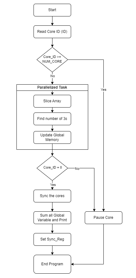
Some key steps required for the multi-core system are provided in the template program. You need to uncomment them after you have finished the modifications in my_system.py.
You need to divide the array between the cores to optimize the core useage. And print the final result correctly.
To run your program you can set the number of cores using:
// Define the number of cores you want to simulate with
#ifndef NUM_CORES
    #define NUM_CORES 1
#endif
Once completed, you can run make all to compile the solution, and make run to execute the solution.
Hint: If you don't see any output in the terminal, check if all the cores are being paused correctly, until Core-0 finishes execution
Verification & Profiling
To verify your program and the core implementation run the following command:
make gvsoc verify
Once the verification is completed successfully you con continue with profiling and answering the questions.
Note: You will need to show the verification output to the TAs during sign-off
Profiling
Set ARRAY 1 and run make plot. This will make a plot between execution-cycles vs. number of cores. Using this plot, answer the following questions:
- Why is the graph non-linear?
- Apply Amdahl's Law on the program using the values in the graph, and calculate the percentage of the code that is parallelizable. You may want to use the following lecture slides: Slide 11
Amdahl's law : $$ Speed up_{max} = {1 \over {(1-p)} + ({p \over s})}$$
Where
- Speed up is the maximum speedup of the system
- p is part of the system that is improved
- s is the speedup of p
- What will be the future trend of the plot if the cores are increased beyond 16?
Set ARRAY 2 and run make diff. The main difference in Array-1 and Array-2 is that there are no 3s in Array-2. Thus you need to analyze how the absence of 3s affects the execution cycles in a multi-core system. To facilitate this analysis, make diff plots the difference in execution cycles for Array-1 and Array-2. Answer the following questions based on your observations of the graph.
- Based on the program in
main.cwhat is the difference in execution for Array-1 and Array-2? - Why is the difference in number of cycles between Array-1 and Array-2 decreasing? Will the difference reach zero if the cores are increased?
- How will the difference change if the number of occurrences are more in Array-1?
Set ARRAY 3 and run make plot. This will make a plot between execution-cycles vs. number of cores. Using this plot, answer the following questions:
- Why is the trend for this plot different from the previous plots?
- For this array what will be the ideal number of cores to execute the program?
BONUS: Run a character histogram algorithm with the multi-core processor
To give everyone a fair chance to check the first two parts, the bonus will only be accepted until 12:30 and after you already signed off Parts 1 and 2.
As the bonus task for this last lab, you will be extending the implementation that you used for Part 2. More specifically, to compute a character histogram. Like the one you did in Lab 3 - Part 3.
First, you need to copy the changes you made to the Part2/my_system.py file to the bonus/my_system.py file. Then, you need to implement the character histogram algorithm in the main.c file, just like you did in Part 2, but taking NUM_BINS into account.
A small and big test arrays are given to you in the main.c file. You can choose to test the program with either of them. The sign off will happen using the big test array.
Once you have implemented the character histogram algorithm, you can run the following command to compile and run the program:
make gvsoc all run
You should see the output of the character histogram in the terminal. To plot and make sure your multi-core implementation is correct, you can run the following command:
make plot
Show your terminal output and the plot to the TAs for the sign-off.
Additional resources
Any additional resources regarding lectures and labs can be found on this page. They will be added throughout the duration of the course.
Lab 1: Introduction to Vivado / Verilog
Lab 2: RISC-V
- PICORV32 Core Repo: YosysHQ/picorv32
- PICORV32 Analysis (Not an official source): Analyze PicoRV32
- RISC-V Instruction Guide: RISCV_CARD
- RISC-V Online Compiler: RISC-V Online Assembler
RISC-V Register Map
| 5-bit Encoding (rx) | Register | ABI Name | Description |
|---|---|---|---|
| 0 (0b00000) | x0 | zero | hardwired zero |
| 1 (0b00001) | x1 | ra | return address |
| 2 (0b00010) | x2 | sp | stack pointer |
| 3 (0b00011) | x3 | gp | global pointer |
| 4 (0b00100) | x4 | tp | thread pointer |
| 5 (0b00101) | x5 | t0 | temporary register 0 |
| 6 (0b00110) | x6 | t1 | temporary register 1 |
| 7 (0b00111) | x7 | t2 | temporary register 2 |
| 8 (0b01000) | x8 | s0 | saved register 0 |
| 9 (0b01001) | x9 | s1 | saved register 1 |
| 10 (0b01010) | x10 | a0 | function argument 0 |
| 11 (0b01011) | x11 | a1 | function argument 1 |
| 12 (0b01100) | x12 | a2 | function argument 2 |
| 13 (0b01101) | x13 | a3 | function argument 3 |
| 14 (0b01110) | x14 | a4 | function argument 4 |
| 15 (0b01111) | x15 | a5 | function argument 5 |
| 16 (0b10000) | x16 | a6 | function argument 6 |
| 17 (0b10001) | x17 | a7 | function argument 7 |
| 18 (0b10010) | x18 | s2 | saved register 2 |
| 19 (0b10011) | x19 | s3 | saved register 3 |
| 20 (0b10100) | x20 | s4 | saved register 4 |
| 21 (0b10101) | x21 | s5 | saved register 5 |
| 22 (0b10110) | x22 | s6 | saved register 6 |
| 23 (0b10111) | x23 | s7 | saved register 7 |
| 24 (0b11000) | x24 | s8 | saved register 8 |
| 25 (0b11001) | x25 | s9 | saved register 9 |
| 26 (0b11010) | x26 | s10 | saved register 10 |
| 27 (0b11011) | x27 | s11 | saved register 11 |
| 28 (0b11100) | x28 | t3 | temporary register 3 |
| 29 (0b11101) | x29 | t4 | temporary register 4 |
| 30 (0b11110) | x30 | t5 | temporary register 5 |
| 31 (0b11111) | x31 | t6 | temporary register 6 |
Area Utilization
To open the area utilization report follow the following steps:
- Ensure that you have a Generated Bitstream
Open Implemented Design, select this above the Generate Bitstream- Select
Report Utilization - Navigate till you see the
picorv32_0
The steps are highlighted below in the picture:

Using the Desktop
Your group can use the desktops in the labs to generate the bitstream. However, some of the desktops cannot be used to program the FPGA. If you need to use the desktops, come to the front of the room, where te first two rows of computers should support programming the FPGA.
To use the desktop follow the steps:
- Login with your NetID and password
- Download the part files from here: No longer available
- Extract the file into
C:\Programs\Xilinx2023.2\Vivado\2023.2\data\parts\xilinx - You can start Vivado and open the template project
- Make sure that you do not get any warnings when you open the template. If you get any errors please contact a TA
Flashing FPGA from the Desktop
The Desktop PCs do not have Vitis CLassic Installed on them. Thus you will be using a custom python script to flash the FPGAs. The script can be downloaded from here: Auto_Upload_Script.
To use the script, follow the steps:
- Unzip the script
- Replace the
design_1_wrapper.bitwith your generated bitstream - Double-click on
run_script.pyto execute the script
Ensure that you open a Serial Port before running the script
Running Remotely
For groups that cannot upload the program onto the FPGA, please upload your Exported Hardware file (*.xsa) to your groups OneDrive folder here: No longer available
Once uploaded there will be TA laptops placed at the front of the Lab for you to upload your program from.
Note: This can be a bottle-neck if many groups want to test their design at the same time. So please keep that in mind and work efficiently. Such as using the desktops in front of the class.
Lab 3: CUDA
Template download
Download the template used for lab 3 here: lab3-cuda-template
List of useful commands on DelftBlue
- See your if your job sits in the queue:
squeue -u $USER - See the job queue:
squeue