The Communication Protocol
All platform components communicate among themselves using the Advanced eXtensible Interface (AXI) protocol, which is a standard ARM communication protocol, and the de facto standard adopted by Xilinx for the connection of IPs and functional blocks in SoC designs. There are 3 types of AXI interfaces employed in the SoC platform:
- AXI3 (component 7 - S_AXI_HP0 port)
- AXI4LITE (component 8 - axi port)
- AXI4 for the rest of the platform components
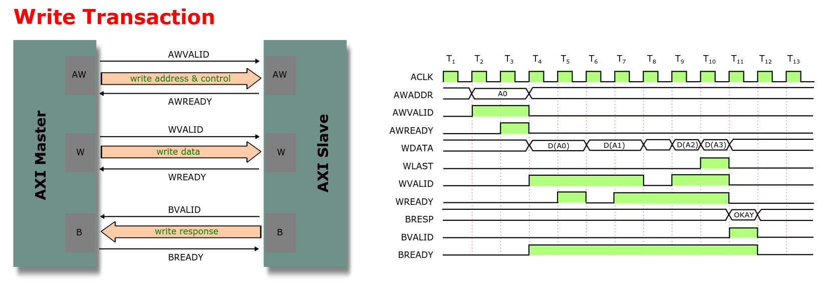
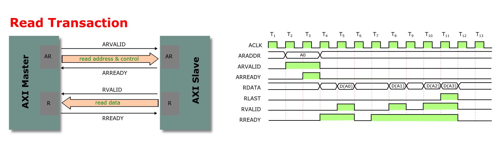
The figure below outlines the AXI4 protocol, architecture and a timing diagram corresponding to a write and a read transaction. Subsequently, we detail only the write transaction handshaking, as the read transaction follows suit. Whenever an AXI Master wants to perform a write transaction, it will send first a set of initial information about the transaction (e.g., burst type, burst size, cacheable attributes of transaction) to the AXI Slave.
At the same time, the AXI Master will send to the AXI Slave the address where the data should be written (AWADDR) and will signal that the driven address is valid (AWVALID). When the AXI Slave is able to accept the address, it will signal back to the AXI Master (AWREADY). The address tranfer from Master to Slave happens when both AWVALID and AWREADY are asserted (clock cycle T3 in the Figure). Similarly to the write address transfer, the write data (WDATA) will be sent from the AXI Master to the AXI Slave (clock cycle T5, T7, T9, and T10 in the Figure). The signal WLAST will mark the last data transfer in the burst. The slave will then respond to the Master if the write transaction was successful or not (BRESP), and assert BVALID when it drives a valid write response (clock cycle T11 in the Figure).