Processor Evaluation
Once you obtain a bug free design you may proceed to its evaluation. Some information can be found in the reports of vivado, such as the maximum operating frequency and the area of your design. Other results can only be found by executing benchmarks on the actual FPGA.
Area Evaluation
Below, an example of a design floorplan is given. This is the design floorplan of the baseline CPU we gave you, with the Programmable Logic (PL) and the Processing System (PS) sections outlined.
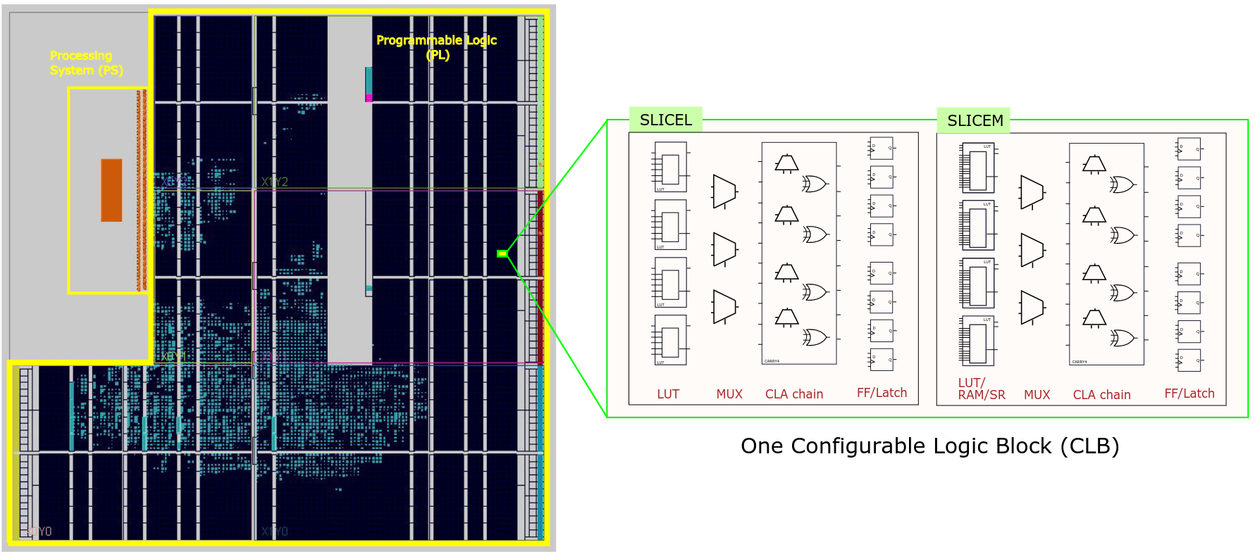
The main resource for combinatorial and sequential circuits are Configurable Logic Blocks (CLBs). Each CLB consists of 2 interconnected slices, as shown in the example above, which contain the following resources:
- 8 look-up tables for random logic implementation or distributed memory,
- 6 multiplexers,
- 2 fast carry chains,
- 16 Flip-Flops out of which 8 can be configured as latches.
For memory implementation, besides the distributed RAM (from CLBs),
a number of 36Kb RAM Blocks (RAMBs) are available
(see Vivado Design Suite 7 Series FPGA and Zynq-7000 SoC Libraries Guide for BRAMs instantiation primitives).
To estimate the area of your design,
a compound value should be derived from the implemented design's Utilization Report.
You can generate this for the cpu_0 component through Vivado's IMPLEMENTATION → Open Implemented Design → Report Utilization.
Below we've shown a sample report of the baseline cpu:
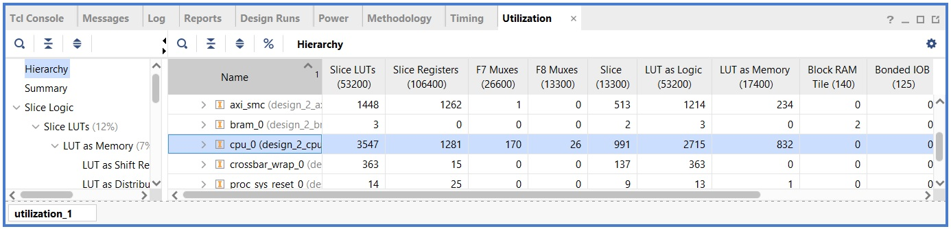
You can then use this information to estimate the total area using the following relations:
- The area of a slice is half the area of a CLB
- The area of a a
RAMB18(18 kbit configurable ram block) is 1.2 times the size of a CLB - The area of a a
RAMB36(36 kbit configurable ram block) is 2.4 times the size of a CLB
In the example from above, cpu_0 doesn't use any block ram tiles,
but 991 slices so the total area is
Timing Analysis
To check that the implemented design works at the requested frequency,
a timing report should be generated in Vivado through IMPLEMENTATION → Open Implemented Design → Report Timing Summary.
A timing tab will open up detailing all the timing constraints
(usually one for each clock signal in the design)
with the top slowest propagation paths and any potential timing violations.
Below, we've shown the timing summary section of the baseline cpu:
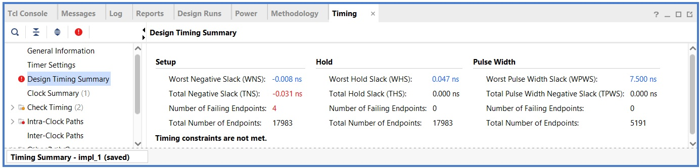
This shows us whether all the timing constraints are met (slack values should be positive to meet timing) and thus that the design will be able to run in a reliable manner at the requested frequency. If the design does not meet the desired frequency, it is recommended to focus on the Worst Negative Slack (WNS) as the main way to improve the total negative slack.
If the slack is positive, the design is guaranteed to work in a reliably at the requested frequency. However, if the slack is negative the design might work within reasonable negative slack bounds, or it might not work properly at all. Based on the WNS value, we can also estimate the maximum attainable operation frequency as follows:
This FMAX estimation could be pessimistic, as Vivado does not try to further improve timing after the timing constraints are met.
Clicking on the value of WNS will display information for the top 10 paths with the worst delay in the design. Double clicking on the critical path (Path 1) will display detailed timing related information, among which the path start point and end point, the number of levels of logic, the logical resources included in the path, and the slack with respect to the requested frequency, as shown below.
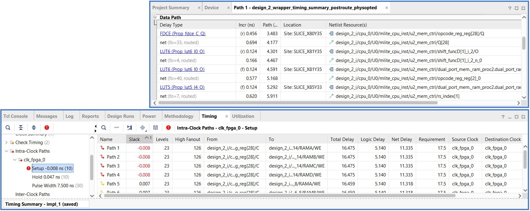
Right-clicking on Path 1, and selecting Schematic will display the critical path schematic, as illustrated.
Further information on how to read a timing report can be found in Vivado documentation
Executing Benchmarks
To evaluate your improvements of the cpu, you are given a set of benchmarks to be run on the FPGA board. After benchmark execution on the board the message "CORRECT!" is displayed if the benchmark results are as expected. Otherwise, an "ERROR" message is displayed.
In addition, to evaluate the performance of your solution, the number of CPU cycles (in million cycles) consumed by the benchmark execution, the peak power consumption (in mW), and the energy (in J) are measured and displayed.
The scores of the baseline cpu for these benchmarks are shown in the table below:
Baseline benchmark scores
| Name | Description | cycles (million) | Time (s) | energy (J) | peak power (mW) |
|---|---|---|---|---|---|
| opcodes | Tests all MIPS I instructions (only for testing) | - | - | - | - |
| cjpeg | JPEG compression | 100.018590 | 1.6952 | 1.722011 | 79.197090 |
| divide | Large number (192Kb) integer division using GMP library | 707.854012 | 11.9975 | 2.467115 | 78.970367 |
| multiply | Large number (64Kb) integer multiplication using GMP library | 390.739735 | 6.6227 | 2.187528 | 81.413025 |
| pi | Computes 1000 digits of PI using basic arithmetic operations | 884.506178 | 14.9916 | 2.784943 | 81.311775 |
| fir | Length-63 bandpass FIR filter applied to 50000 input samples | 213.740789 | 3.6227 | 1.696708 | 72.882149 |
| rsa | RSA message signing using GMP library | 1420.508182 | 24.0764 | 3.230663 | 79.212349 |
| ssd | Pattern matching using Sum-of-Squared-Differences | 2305.992254 | 39.0846 | 4.397920 | 82.596886 |
| ssearch | String search using look-up tables | 1419.875462 | 24.0657 | 3.343137 | 81.810158 |
| susan | Gaussian image smoothing | 1601.722838 | 27.1478 | 3.540810 | 82.110268 |
| benchall | All Benchmarks in one run | 8654.753342 | 146.6907 | 11.774730 | 81.538254 |
The C and assembly source code for each benchmark can be found in the benchmarks folder. Note that if your cpu performance improvement strategy relies (also) on MIPS ISA modification/augmentation, then you need to recompile the benchmarks before running them.
In order to execute the benchmarks on your modified cpu, 2 things are needed:
- the bitstream file (
.bit) (generated in Vivado) which is to be uploaded to the board and used to configure the FPGA - the benchmarks
.binfile.
These two files are stored on the ZYNC's SD card. To manage the benchmarks execution, the ARM cpu on the Zynq board is used. Specifically, the ARM cpu tasks are: initialize the board interfaces, transfer the benchmark from SD card into the DDR memory, start the benchmark execution on the processor, receive the benchmark results from the processor, and redirect them in an external file. The ARM cpu tasks are performed according to a c program created in Vitis.
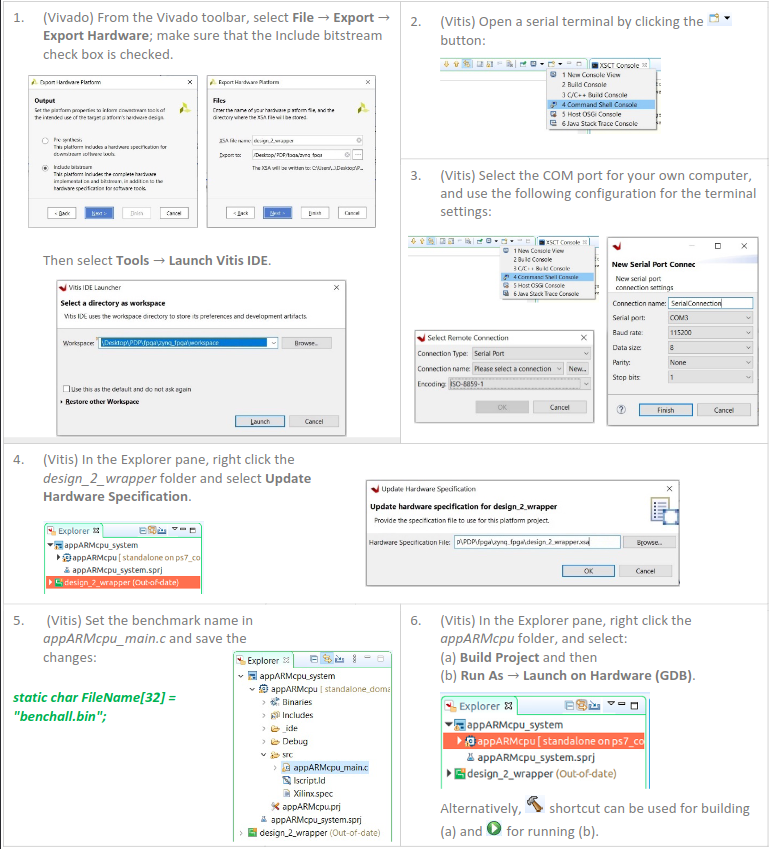
After the bistream generation has completed successfully in Vivado,
you can use the workflow shown below to create a wrapper bitsteam called design_2_wrapper.bit.
The steps below line up with the ones highlighted in the picture below.
- Create a compound file
design_2_wrapper.xsa, which should be infpga/zynq_fpga. This file contains the bitstream and other files necessary for the initialization of comonents like clocks, DDR and GPIO. - You can skip this step when you don't have physical access to the ZYNC like what is the case during this course.
- This one as well.
- Launch vitis and make it aware of the changed hardware specification
design_2_wrapper.xsa. - Next you should change a line in the code that will run on the ARM cpu next to the FPGA. (source code in
appARMcpu_main.c). You should set of the name of the benchmark you want to run. This c program will allow:- To read from the board SD card the target benchmark that will be evaluated on your processor and to transfer it to the PS DDR memory
- To initialize the PS components (clocks, DDR, GPIO), provide the PL clock and reset the PL logic
- to receive the benchmark results from the UART and redirect them to an external file.
- Compile this program through vitis to get an executable:
appARMcpu.elf. Of course you can also skip step 6b since you don't have a board physically connected to your laptop.
You're now done with Vitis, and you can close it.
Running Benchmarks Remotely
The communication of input/output files for remote FPGA access is performed via Dropbox shared folders.
Preliminary Dropbox folder setup:
For each group, a shared folder will be created on dropbox. In order to access the group folder, you are required to have Dropbox (www.dropbox.com) account(s) and provide us with the email addresses linked to your Dropbox accounts. Please send an email to j.b.doenszelmann@tudelft.nl with your group's names and email addresses which are linked to your dropbox accounts. A shared dropbox folder can then be accessed for upload/download either locally (if the Dropbox client is locally installed), or online via the Dropbox website.
The remote access flow for verifying the FPGA implemented design consists of the following steps:
- Place the
design_2_wrapper.xsa(located typically in thefpga/zynq_fpgafolder) andappARMcpu.elf(located in thefpga/zynq_fpga/workspace/appARMcpu/Debugfolder) files in the Dropbox folder. NOTE: Only files with these names are accepted. - The FPGA will be programmed automatically with the bistream
design_2_wrapper.bit, and the ARM cpu prepared for executing theappARMcpu.elfapplication. Afterwards, these files will be automatically deleted from the Dropbox folder. NOTE: There are multiple FPGA boards. The scheduling time for programming each bitstream on an FPGA is compliant with a round robin scheduling policy, relative to the remaining Dropbox groups' folders and the individual bitstream files timestamp. - For each programmed bitstream, two output files will be generated in the Dropbox folder:
- results.txt file with the benchmark execution related results (e.g., status of the benchmark results correctness, performance) – log.txt file consisting of ERRORS/INFO/WARNINGS concerning the status of the enti re simulation (e.g., files consistency, FPGA programming, UART receive/transmit).
In both .txt files, "DONE" marks a successful end of communication with the remote FPGA board.
Warning:
If you want to preserve the .txt files, you have to save them in a separate folder, as the next evaluation will overwrite them.
Custom Benchmarks
For testing a custom benchmark three files have to be placed in the Dropbox folder:
- design_2_wrapper.xsa,
- appARMcpu.elf (after being modified in Vitis to update the benchmark name to ’custom.bin’),
- and a file called
custom.bin(which is generated using the provided MIPS cross-compiler).
Energy Evaluation
The Vivado tool can provide a power consumption estimate of your design,
obtained through IMPLEMENTATION → Open Implemented Design → Report Power.
To derive the dynamic power consumption estimate,
the Vivado tool, by default,
does not require the user to specify any information related to the switching profile of the design nets (default switching rates are being assumed).
The confidence level of this estimate however is relatively low,
and in order to perform a more accurate power analysis,
a profile with the actual implemented design signals switching activity should be provided.
Such a switching profile can be obtained by simulating the implemented design in QuestaSim with a benchmark and logging for the design relevant signals the value changes and their timestamps.
Such a process is very time consuming and the estimates can still suffer from accuracy issues when compared to the actual power consumed when running on the board.
Thus instead, we will monitor and measure the power rails of the PL fabric while running the
benchmark on the board.
Based on these measurements the energy consumption and peak power
are derived.
These values are part of the results displayed in the results.txt file after a successful
benchmark completion.
Note:
QuestaSim is a proprietary tool that you probably cannot get anyway. Testing it on a real board is probably your only option.