Methodology
The first question we need to address is “What do we need in order to improve the system?” Starting from one of your targets, e.g., to improve the computational performance of an arithmetic core, you need at least an Electronic Design Automation (EDA) tool to describe your design by using VHDL. An EDA tool is not just a text editor for VHDL, even though most of the time you’ll be struggling in VHDL, it creates the premises to translate your VHDL description into "real" FPGA hardware.
Then you need to evaluate your design, to check its correctness and efficiency, so you need a way to simulate your design and to map it into real hardware. Moreover you need benchmarks to evaluate its correctness and performance.
Since an arithmetic core cannot run on its own, you need a supporting platform to embed it in, and on this platform you can execute the benchmark programs. This platform should be easily implementable in the same way in which your designs are going to be implemented. Concerning the benchmarks, you can develop them by yourself to verify your design, or you can use standard generally acceptable sets to evaluate your design and then to compare it with equivalent counterparts. The benchmark programs are usually written in a programming language with little runtime overhead, like C or Rust for example.
Generally speaking, the supporting system on which the implementation tools and the benchmark compilation are run on, has another instruction set than the general-purpose processor for which you develop your project. Thus you need a dedicated compiler (a "cross compiler" as the target platform is different than the host platform) to compile the benchmark programs for the supporting platform. Once you get the EDA tools, the supporting processor, implement the required hardware, and generate the benchmarks binary via compilation, you can start evaluating your design.
In the best scenario you can simulate your design and synthesize it without any errors or bugs. In that case you can carry on the evaluation and if the obtained performance is satisfactory you can start writing your report. However this is quite unlikely to happen after the first attempt. Most of the time, you will get fatal errors at compilation time, soft errors at execution time, or some strange errors you don’t have a clue where they are coming from. In any of these cases, you need some debugging tools, for hardware or software, and/or for both of them.
FPGA work
Work with an actual FPGA is done remotely. To do so, you should make sure we have you email address that is linked to a dropbox account. More information can be found here.
Project Workflow
To design, debug, and evaluate your improved processor you have to synthesize it on an FPGA board. For that you should follow the following workflow:
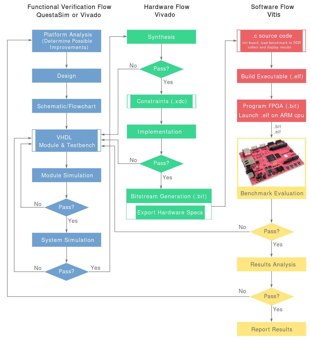
In the project you will follow these steps:
- The baseline design (the reference design that you will receive) should be analyzed and its weak point(s) determined by means of, e.g., profiling.
- Avenues for improvement should be identified.
- For each processor component you want to add or change, you should make a pen-and-paper plan capturing its input and output ports and RTL design.
- Write the corresponding HDL code for that component and test whether it performs its function as intended or not (behavioral RTL simulation).
- Only then, you can test the design on the FPG. For that the following steps need to be taken
- Logic synthesis, converting the RTL constructs from the HDL code into a design implementation in terms of generic resources (LUTs, MUXes, memory, flip-flops, adders, etc.).
- Map the design generic resources into the specific resources available on the Zynq FPGA (e.g., slices, IOBs)
- "Place and Route", wiring components together, such that the design criteria imposed (such as pin constraints for components ports and timing constraaints) are being met.
- Load the resulting "bit file" onto the FPGA, to test.
Behavioral testing
Generally speaking, it is advisable to write a HDL testbench and test each component individually, before integrating it inside the system. A bit like unit tests in software.
The alternative would be to opt for testing the entire system, maybe through the c programs we provide. Though possible, it will be harder to debug your design that way.
To evaluate your processor, a set of benchmarks will be executed. A software application that will initialize the board, send the benchmark to the DDR memory, and finally collect the benchmark results from the board and further display them is also required.
This application can be executed on your computer, to test in the provided emulator. However, once you uploaded the bitstream to the FPGA board, the same code can be executed there, since the board also incorporates an ARM processor. The system timing performance, area, and energy consumption can now be evaluated and appropriate further actions undertaken.
While doing this project, we strongly recommend that you do the following:
- Make a clear plan for your design before you start writing VHDL code.
- Run a module level simulation every time you modify something in your VHDL code, before you start running a system level simulation.
- Run a system simulation every time you change your design before you synthesize it!
- Put your source code in git, so that you can restore old versions.